SLLSFC2D December 2020 – September 2021 ISO1640 , ISO1641 , ISO1642 , ISO1643 , ISO1644
PRODUCTION DATA
- 1 Features
- 2 Applications
- 3 Description
- 4 Revision History
- 5 Pin Configuration and Functions
-
6 Specifications
- 6.1 Absolute Maximum Ratings
- 6.2 ESD Ratings
- 6.3 Recommended Operating Conditions
- 6.4 Thermal Information
- 6.5 Power Ratings
- 6.6 Insulation Specifications
- 6.7 Safety-Related Certifications
- 6.8 Safety Limiting Values
- 6.9 Electrical Characteristics
- 6.10 Supply Current Characteristics
- 6.11 Timing Requirements
- 6.12 I2C Switching Characteristics
- 6.13 GPIO Switching Characteristics
- 6.14 Insulation Characteristics Curves
- 6.15 Typical Characteristics
- 7 Parameter Measurement Information
- 8 Detailed Description
- 9 Application and Implementation
- 10Power Supply Recommendations
- 11Layout
- 12Device and Documentation Support
- 13Mechanical, Packaging, and Orderable Information
5 Pin Configuration and Functions
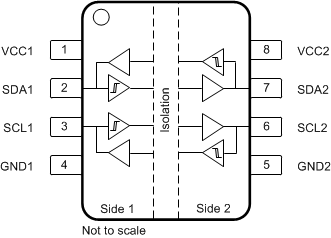 Figure 5-1 ISO1640B Package8-Pin SOICTop View
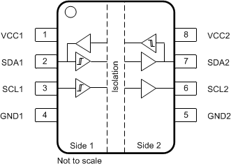 Figure 5-2 ISO1641B Package8-Pin
SOICTop View
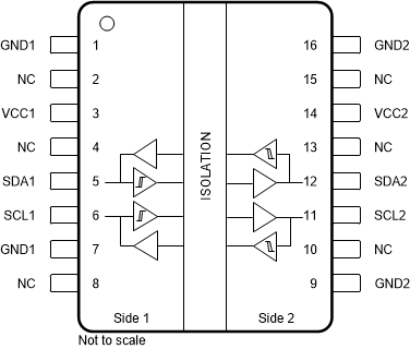 Figure 5-3 ISO1640 Package16-Pin SOICTop
View
Figure 5-4 ISO1641 Package16-Pin
SOICTop View
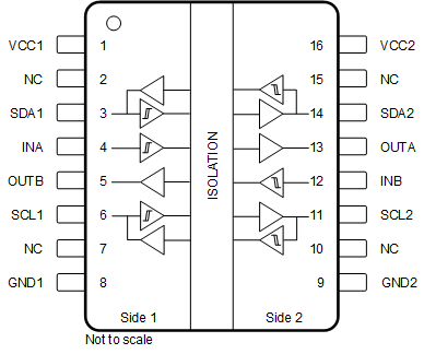 Figure 5-5 ISO1642 Package16-Pin SOICTop
View
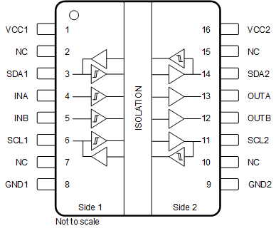 Figure 5-6 ISO1643 Package16-Pin SOICTop
View
Figure 5-7
ISO1644 Package16-Pin SOICTop View
Table 5-1 Pin Functions — ISO1640 and ISO1641
| PIN | I/O | DESCRIPTION | ||
|---|---|---|---|---|
| 8-D | 16-DW | |||
| NAME | NO. | NO. | ||
| GND1 | 4 | 1, 7 | — | Ground, side 1 |
| GND2 | 5 | 9, 16 | — | Ground, side 2 |
| NC | — | 2, 4, 8, 10, 13, 15 | — | No Connection |
| SCL1 | 3 | 6 | I/O | Serial clock input / output, side 1 (ISO1640 only) Serial clock input, side 1 (ISO1641 only) |
| SCL2 | 6 | 11 | I/O | Serial clock input / output, side 2 (ISO1640 only) Serial clock output, side 2 (ISO1641 only) |
| SDA1 | 2 | 5 | I/O | Serial data input / output, side 1 |
| SDA2 | 7 | 12 | I/O | Serial data input / output, side 2 |
| VCC1 | 1 | 3 | — | Supply voltage, side 1 |
| VCC2 | 8 | 14 | — | Supply voltage, side 2 |
Table 5-2 Pin Functions — ISO1642 and ISO1643
| PIN | I/O | DESCRIPTION | |
|---|---|---|---|
| 16-DW | |||
| NAME | NO. | ||
| GND1 | 8 | — | Ground, side 1 |
| GND2 | 9 | — | Ground, side 2 |
| INA | 4 | I | Input, channel A |
| INB/OUTB | 12 | — | Input, channel B (ISO1642) Output, channel B (ISO1643) |
| NC | 2, 7, 10, 15 | — | No Connect |
| OUTA | 13 | O | Output, channel A |
| OUTB/INB | 5 | — | Output, channel B (ISO1642) Input, channel B (ISO1643) |
| SCL1 | 6 | I/O | Serial clock input / output, side 1 |
| SCL2 | 11 | I/O | Serial clock input / output, side 2 |
| SDA1 | 3 | I/O | Serial data input / output, side 1 |
| SDA2 | 14 | I/O | Serial data input / output, side 2 |
| VCC1 | 1 | — | Supply voltage, side 1 |
| VCC2 | 16 | — | Supply voltage, side 2 |
Table 5-3 Pin Functions — ISO1644
| PIN | I/O | DESCRIPTION | |
|---|---|---|---|
| 16-DW | |||
| NAME | NO. | ||
| GND1 | 2, 8 | — | Ground, side 1 |
| GND2 | 9, 15 | — | Ground, side 2 |
| INA | 4 | I | Input, channel A |
| INB | 5 | I | Input, channel B |
| INC | 10 | I | Input, channel C |
| OUTA | 13 | O | Output, channel A |
| OUTB | 12 | O | Output, channel B |
| OUTC | 7 | O | Output, channel C |
| SCL1 | 6 | I/O | Serial clock input / output, side 1 |
| SCL2 | 11 | I/O | Serial clock input / output, side 2 |
| SDA1 | 3 | I/O | Serial data input / output, side 1 |
| SDA2 | 14 | I/O | Serial data input / output, side 2 |
| VCC1 | 1 | — | Supply voltage, side 1 |
| VCC2 | 16 | — | Supply voltage, side 2 |