ZHCSIE0A June 2018 – October 2018 ISO224
PRODUCTION DATA.
- 1 特性
- 2 应用
- 3 说明
- 4 修订历史记录
- 5 器件比较表
- 6 Pin Configuration and Functions
-
7 Specifications
- 7.1 Absolute Maximum Ratings
- 7.2 ESD Ratings
- 7.3 Recommended Operating Conditions
- 7.4 Thermal Information
- 7.5 Power Ratings
- 7.6 Insulation Specifications
- 7.7 Safety-Related Certifications
- 7.8 Safety Limiting Values
- 7.9 Electrical Characteristics
- 7.10 Switching Characteristics
- 7.11 Insulation Characteristics Curves
- 7.12 Typical Characteristics
- 8 Detailed Description
- 9 Application and Implementation
- 10Power Supply Recommendations
- 11Layout
- 12器件和文档支持
- 13机械、封装和可订购信息
8.3.1 Analog Input
The input stage of the ISO224 feeds a switched capacitor, feed-forward ΔΣ modulator. The modulator converts the analog signal into a bitstream that is transferred over the isolation barrier, as described in the Isolation Channel Signal Transmission section. The high-impedance and low bias-current input of the ISO224 makes the device suitable for isolated voltage sensing applications.
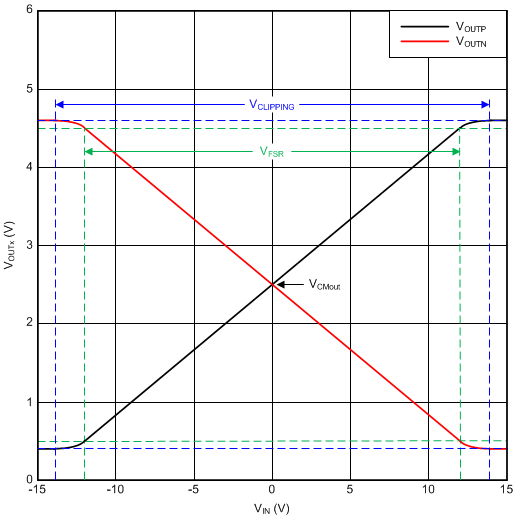
Figure 41 visualizes the difference in the transfer function of the ISO224 depending on the input signal VIN, as specified in the Recommended Operating Conditions table. With the input voltage within the specified full-scale range VFSR, the output of the device changes in a linear way with small error as specified by the nonlinearity parameter in the Electrical Characteristics table. If the input signal exceeds the VFSR range, the nonlinearity of the output signals increases and the amplitude clips at VIN = VCLIPPING.
 Figure 41. Transfer Function of the ISO224
 There are two restrictions on the analog input signal at the IN pin. First, if the input voltage VIN exceeds the range of –15 V to 15 V, the current must be limited to 10 mA to prevent damage to the input clamp, see the Input Clamp Protection Circuit section for further information. In addition, the linearity and noise performance of the ISO224 are ensured only when the analog input voltage remains within the specified linear full-scale range (VFSR).