ZHCS029E January 2011 – August 2023 ISO3086T
PRODUCTION DATA
- 1
- 1 特性
- 2 应用
- 3 说明
- 4 Revision History
- 5 Pin Configuration and Functions
-
6 Specifications
- 6.1 Absolute Maximum Ratings
- 6.2 ESD Ratings
- 6.3 Recommended Operating Conditions
- 6.4 Thermal Information
- 6.5 Power Ratings
- 6.6 Insulation Specifications
- 6.7 Safety-Related Certifications
- 6.8 Safety Limiting Values
- 6.9 Electrical Characteristics: Driver
- 6.10 Electrical Characteristics: Receiver
- 6.11 Transformer Driver Characteristics
- 6.12 Supply Current
- 6.13 Switching Characteristics: Driver
- 6.14 Switching Characteristics: Receiver
- 6.15 Insulation Characteristics Curves
- 6.16 Typical Characteristics
- 7 Parameter Measurement Information
- 8 Detailed Description
- 9 Application and Implementation
- 10Power Supply Recommendations
- 11Layout
- 12Device and Documentation Support
- 13Mechanical, Packaging, and Orderable Information
6.16 Typical Characteristics

| TA = 25 °C | PRBS Data 216 - 1 |

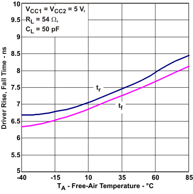
| VCC1 = VCC2 = 5 V | CL = 50 pF | RL = 54 Ω |

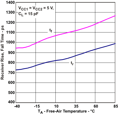
| VCC1 = VCC2 = 5 V | CL = 15 pF |
 Figure 6-8 Driver Rise, Fall Time vs Free-Air Temperature
 Figure 6-10 Receiver Rise, Fall Time vs Free-Air Temperature
| TA = 25 °C |

| TA = 25 °C | VCC1 = 5 V |

| TA = 25 °C | RL = 54 Ω |

| TA = 25 °C | Receiver CL = 15 pF | PRBS Data 216 - 1 |
| Driver CL = 50 pF | Driver RL = 54 Ω |

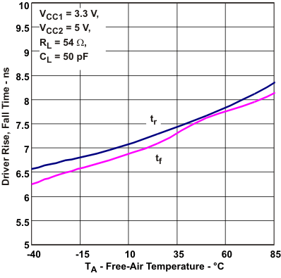
| VCC1 = 3.3V, VCC2 = 5 V | CL = 50 pF | RL = 54 Ω |

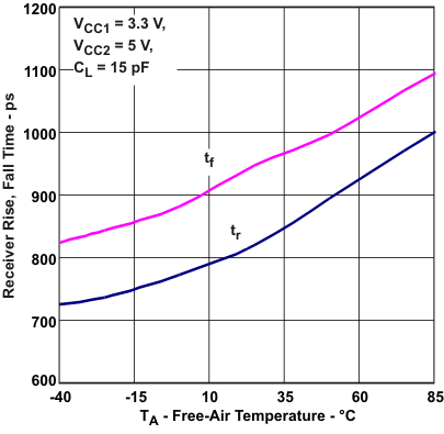
| VCC1 = 3.3V, VCC2 = 5 V | CL = 15 pF | RL = 54 Ω |
 Figure 6-9 Driver Rise, Fall Time vs Free-Air Temperature
 Figure 6-11 Receiver Rise, Fall Time vs Free-Air Temperature
| TA = 25 °C | VCC1 = 5 V |

| TA = 25 °C | VCC1 = 5 V |
 Figure 6-17 Recommended Minimum Differential Input Voltage vs Signaling Rate