ZHCSSZ3H May 2008 – August 2023 ISO15 , ISO35
PRODUCTION DATA
- 1
- 1 特性
- 2 应用
- 3 说明
- 4 Revision History
- 5 Pin Configuration and Functions
-
6 Specifications
- 6.1 Absolute Maximum Ratings
- 6.2 ESD Ratings
- 6.3 Recommended Operating Conditions
- 6.4 Thermal Information
- 6.5 Power Ratings
- 6.6 Insulation Specifications
- 6.7 Safety-Related Certifications
- 6.8 Safety Limiting Values
- 6.9 Electrical Characteristics: Driver
- 6.10 Electrical Characteristics: Receiver
- 6.11 Supply Current
- 6.12 Switching Characteristics: Driver
- 6.13 Switching Characteristics: Receiver
- 6.14 Insulation Characteristics Curves
- 6.15 Typical Characteristics
- 7 Parameter Measurement Information
- 8 Detailed Description
- 9 Application and Implementation
- Power Supply Recommendations
- 10Layout
- 11Device and Documentation Support
- 13Mechanical, Packaging, and Orderable Information
5 Pin Configuration and Functions
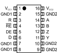
 Figure 5-1 ISO35x DW Package
16-Pin SOIC
Top View
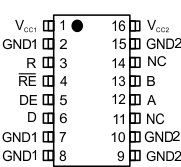
 Figure 5-2 ISO15x DW Package
16-Pin SOIC
Top View
Table 5-1 Pin Functions
| PIN | I/O | DESCRIPTION | ||
|---|---|---|---|---|
| NAME | ISO15x NO. |
ISO35x NO. |
||
| A | 12 | 14 | I/O | ISO15x: Noninverting bus input or output |
| I | ISO35x: Noninverting bus input | |||
| B | 13 | 13 | I/O | ISO15x: Inverting bus input or output |
| I | ISO35x: Inverting bus input | |||
| D | 6 | 6 | I | Driver input |
| DE | 5 | 5 | I | Driver logic-high enable input |
| GND1 | 2,7,8 | 2,7,8 | — | Logic side ground; internally connected |
| GND2 | 9,10,15 | 9,10,15 | — | Bus side ground; internally connected |
| NC | 11,14 | — | — | Not connected internally; may be left floating |
| R | 3 | 3 | O | Receiver output |
| RE | 4 | 4 | I | Receiver logic-low enable |
| VCC1 | 1 | 1 | — | Logic side power supply |
| VCC2 | 16 | 16 | — | Bus side power supply |
| Y | — | 11 | O | Noninverting bus output |
| Z | — | 12 | O | Inverting bus output |