ZHCSE64C august   2015  – may 2023 ISO5452

PRODUCTION DATA  

  1.   1
  2. 特性
  3. 应用
  4. 说明
  5. Revision History
  6. 说明(续)
  7. Pin Configuration and Function
  8. Specifications
    1. 7.1  Absolute Maximum Ratings
    2. 7.2  ESD Ratings
    3. 7.3  Recommended Operating Conditions
    4. 7.4  Thermal Information
    5. 7.5  Power Ratings
    6. 7.6  Insulation Specifications
    7. 7.7  Safety-Related Certifications
    8. 7.8  Safety Limiting Values
    9. 7.9  Electrical Characteristics
    10. 7.10 Switching Characteristics
    11. 7.11 Insulation Characteristics Curves
    12. 7.12 Typical Characteristics
  9. Parameter Measurement Information
  10. Detailed Description
    1. 9.1 Overview
    2. 9.2 Functional Block Diagram
    3. 9.3 Feature Description
      1. 9.3.1 Supply and Active Miller Clamp
      2. 9.3.2 Active Output Pull-down
      3. 9.3.3 Undervoltage Lockout (UVLO) with Ready (RDY) Pin Indication Output
      4. 9.3.4 Soft Turn-Off, Fault ( FLT) and Reset ( RST)
      5. 9.3.5 Short Circuit Clamp
    4. 9.4 Device Functional Modes
  11. 10Application and Implementation
    1. 10.1 Application Information
    2. 10.2 Typical Applications
      1. 10.2.1 Design Requirements
      2. 10.2.2 Detailed Design Procedure
        1. 10.2.2.1  Recommended ISO5452 Application Circuit
        2. 10.2.2.2  FLT and RDY Pin Circuitry
        3. 10.2.2.3  Driving the Control Inputs
        4. 10.2.2.4  Local Shutdown and Reset
        5. 10.2.2.5  Global-Shutdown and Reset
        6. 10.2.2.6  Auto-Reset
        7. 10.2.2.7  DESAT Pin Protection
        8. 10.2.2.8  DESAT Diode and DESAT Threshold
        9. 10.2.2.9  Determining the Maximum Available, Dynamic Output Power, POD-max
        10. 10.2.2.10 Example
        11. 10.2.2.11 Higher Output Current Using an External Current Buffer
      3. 10.2.3 Application Curves
  12. 11Power Supply Recommendations
  13. 12Layout
    1. 12.1 Layout Guidelines
    2. 12.2 Layout Example
    3. 12.3 PCB Material
  14. 13Device and Documentation Support
    1. 13.1 Device Support
      1. 13.1.1 第三方米6体育平台手机版_好二三四免责声明
    2. 13.2 Documentation Support
      1. 13.2.1 Related Documentation
    3. 13.3 接收文档更新通知
    4. 13.4 支持资源
    5. 13.5 Trademarks
    6. 13.6 静电放电警告
    7. 13.7 术语表
  15. 14Mechanical, Packaging, and Orderable Information

封装选项

请参考 PDF 数据表获取器件具体的封装图。

机械数据 (封装 | 引脚)
  • DW|16
散热焊盘机械数据 (封装 | 引脚)
订购信息

Typical Characteristics

GUID-0CF762F2-E6F0-4A65-8B7C-E85B40E7AD4F-low.gif
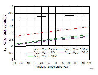
Figure 7-4 Output High Drive Current vs Temperature
GUID-A01DBE0F-0039-4C20-9EF6-70BBDCE349A0-low.gif
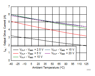
Figure 7-6 Output Low Drive Current vs Temperature
GUID-14B10082-9D3C-4B0A-BFB8-5C0CCEF54EE6-low.gif
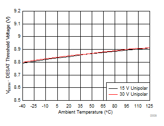
Unipolar: VCC2 – VEE2 = VCC2 – GND2
Figure 7-8 DESAT Threshold Voltage vs Temperature
GUID-0CF73B43-BCFC-46D9-9823-7E4A21A2FC10-low.gif
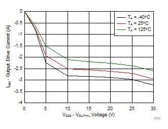
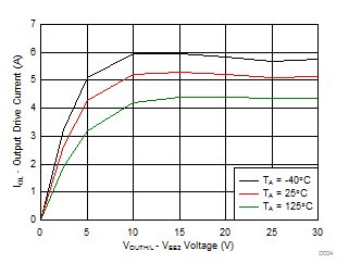
Figure 7-5 Output High Drive Current vs Output Voltage
GUID-7B56A960-44FE-4C9F-92A4-2E9BBE1A2D9C-low.gif
Figure 7-7 Output Low Drive Current vs Output Voltage
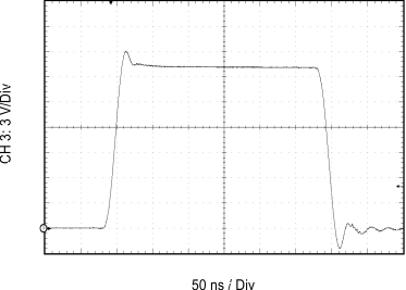
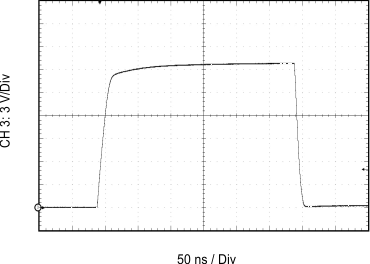
GUID-4D3922EE-E3ED-467F-B8F4-C10F2AB14672-low.gif
CL = 1 nFRGH = 0 ΩRGL = 0 Ω
VCC2 – VEE2 = VCC2 – GND2 = 20 V
Figure 7-9 Output Transient Waveform
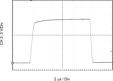
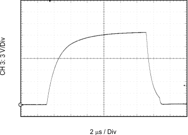
GUID-8B5A3D76-16DC-4A1A-B55F-13836B132C51-low.gif
CL = 100 nFRGH = 0 ΩRGL = 0 Ω
VCC2 – VEE2 = VCC2 – GND2 = 20 V
Figure 7-11 Output Transient Waveform
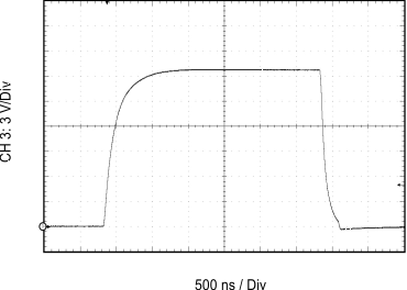
GUID-279D0545-8256-4D36-9340-4348FA0EBBF2-low.gif
CL = 10 nFRGH = 10 ΩRGL = 5Ω
VCC2 – VEE2 = VCC2 – GND2 = 20 V
Figure 7-13 Output Transient Waveform
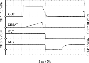
GUID-CD11AA96-B8B0-40C4-8197-47111CEBFCFB-low.gif
CL = 10 nFRGH = 0 ΩRGL = 0 Ω
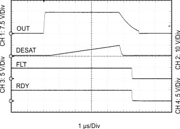
VCC2 – VEE2 = VCC2 – GND2 = 15 VDESAT = 220pF
Figure 7-15 Output Transient Waveform DESAT, RDY and FLT
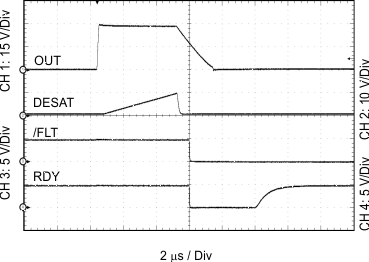
GUID-F8EE3369-9119-47F5-83F6-F46F1A7EB23B-low.gif
CL = 10 nFRGH = 0 ΩRGL = 0 Ω
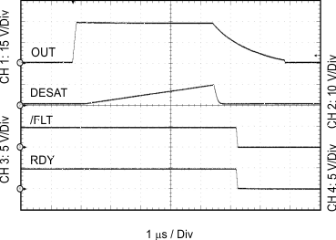
VCC2 – VEE2 = VCC2 – GND2 = 30 VDESAT = 220pF
Figure 7-17 Output Transient Waveform DESAT, RDY and FLT
GUID-431CBC18-3189-40B3-852C-654781D2EE46-low.gif
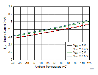
IN+ = HighIN– = Low
Figure 7-19 ICC1 Supply Current vs Temperature
GUID-FBE0C16E-6544-4C36-8D5A-6D1DD166FDDD-low.gif
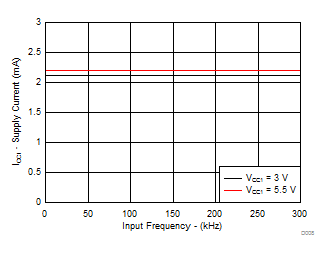
Figure 7-21 ICC1 Supply Current vs Input Frequency
GUID-00F92ED0-476B-453E-AB60-19D48B48EDEE-low.gif
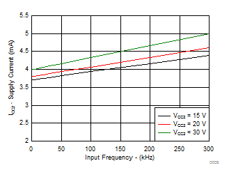
No CL
Figure 7-23 ICC2 Supply Current vs Input Frequency
GUID-C7F41ADA-144A-4A1D-B686-3A04DC4EC00C-low.gif
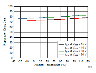
CL = 1 nFRGH = 0 ΩRGL = 0 Ω
VCC1 = 5 V
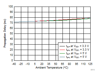
Figure 7-25 Propagation Delay vs Temperature
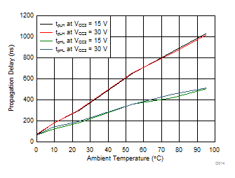
GUID-7D5880EB-A112-46FB-A502-0E5AF481089B-low.gif
RGH = 10 ΩRGL = 5 ΩVCC1 = 5 V
Figure 7-27 Propagation Delay vs Load Capacitance
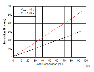
GUID-427B641B-A6C6-43B4-8AF5-8B8B32336051-low.gif
RGH = 0 ΩRGL = 0 ΩVCC1 = 5 V
Figure 7-29 tf Fall Time v. Load Capacitance
GUID-8A3213D2-6830-4DF2-B437-469AEE380765-low.gif
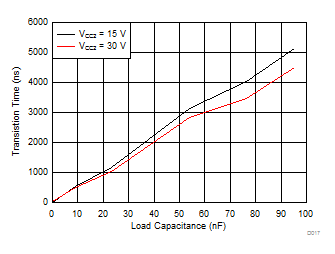
RGH = 10 ΩRGL = 5 ΩVCC1 = 5 V
Figure 7-31 tf Fall Time vs Load Capacitance
GUID-D3E91CBE-DBBF-4EDB-9E63-720B8D80A502-low.gif
CL = 10 nFRGH = 0 ΩRGL = 0 Ω
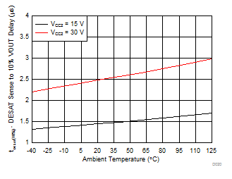
Figure 7-33 DESAT Sense to VOUTH/L 10% Delay vs Temperature
GUID-29C7901B-EF40-4CDE-9234-E5A6844A9B06-low.gif
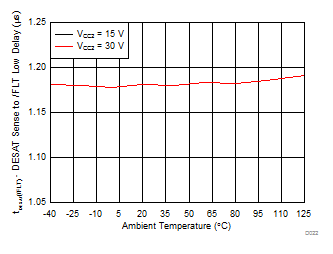
Figure 7-35 DESAT Sense to Fault Low Delay vs Temperature
GUID-E7AAA22E-E215-4C22-94CB-11ABB083F3F3-low.gif
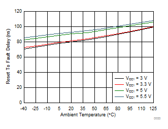
Figure 7-37 Reset to Fault Delay Across Temperature
GUID-0213E161-72AC-48AF-B6CA-E2C5C7EAE38E-low.gif
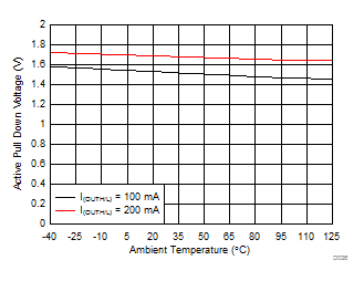
Figure 7-39 Active Pull Down Voltage vs Temperature
GUID-D7C2AB76-3D76-4F10-B4E9-E1535A69BF22-low.gif
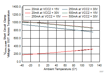
Figure 7-41 VOUTH_CLAMP - Short Circuit Clamp Voltage on OUTH Across Temperature
GUID-392602E0-FF4A-4FD7-951F-5C83C73E5F8A-low.gif
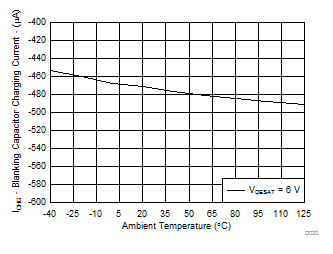
VCC2 = 15 VDESAT = 6 V
Figure 7-43 Blanking Capacitor Charging Current vs Temperature
GUID-F3853DF5-2C16-4F52-B3D8-C7A518635817-low.gif
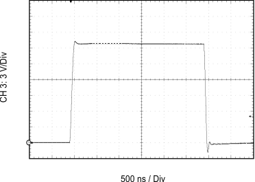
CL = 10 nFRGH = 0 ΩRGL = 0 Ω
VCC2 – VEE2 = VCC2 – GND2 = 20 V
Figure 7-10 Output Transient Waveform
GUID-233BC2B3-999B-43CF-BD2A-769DDF1B4500-low.gif
CL = 1 nFRGH = 10 ΩRGL = 5Ω
VCC2 – VEE2 = VCC2 – GND2 = 20 V
Figure 7-12 Output Transient Waveform
GUID-F74EE148-2C78-43D0-AF0D-C00E015D49DF-low.gif
CL = 100 nFRGH = 10 ΩRGL = 5Ω
VCC2 – VEE2 = VCC2 – GND2 = 20 V
Figure 7-14 Output Transient Waveform
GUID-2DE6D646-F9BF-4992-8FCB-0DD60B00836E-low.gif
CL = 10 nFRGH = 0 ΩRGL = 0 Ω
VCC2 – VEE2 = VCC2 – GND2 = 15 VDESAT = 220pF
Figure 7-16 Output Transient Waveform DESAT, RDY and FLT
GUID-E6B77D51-543D-48FB-A2DA-D106BC5BE8EE-low.gif
CL = 10 nFRGH = 0 ΩRGL = 0 Ω
VCC2 – VEE2 = VCC2 – GND2 = 30 VDESAT = 220pF
Figure 7-18 Output Transient Waveform DESAT, RDY and FLT
GUID-888F40CA-0320-4AF9-BAB6-506D3D7A9972-low.gif
IN+ = LowIN– = Low
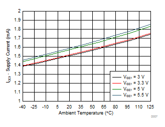
Figure 7-20 ICC1 Supply Current vs Temperature
GUID-6D903F8F-633C-43ED-A358-BD19EEC1C357-low.gif
Input frequency = 1 kHz
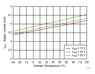
Figure 7-22 ICC2 Supply Current vs Temperature
GUID-9884606E-7116-4F5D-8B73-D3E71508634C-low.gif
RGH = 10 ΩRGL = 5 Ω, 20 kHz
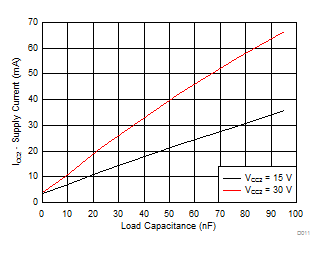
Figure 7-24 ICC2 Supply Current vs Load Capacitance
GUID-94C41A0C-6209-4D94-882E-99432A272B66-low.gif
CL = 1 nFRGH = 0 ΩRGL = 0 Ω
VCC2 = 15 V
Figure 7-26 Propagation Delay vs Temperature
GUID-49DD3C8A-EAF9-490D-AC1C-314E86E5DDBB-low.gif
RGH = 0 ΩRGL = 0 ΩVCC1 = 5 V
Figure 7-28 tr Rise Time vs Load Capacitance
GUID-5D6A3C4F-9FBD-4C2A-A8BD-41DD2CD5DA05-low.gif
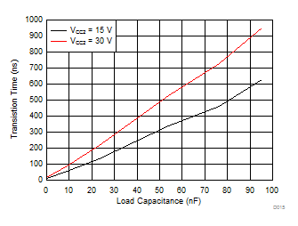
RGH = 10 ΩRGL = 5 ΩVCC1 = 5 V
Figure 7-30 tr Rise Time vs Load Capacitance
GUID-6C57ADBB-2626-4514-A4D2-38A1F8DA97CE-low.gif
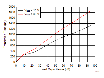
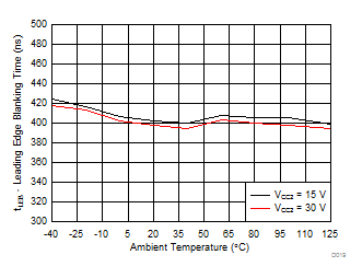
Figure 7-32 Leading Edge Blanking Time With Temperature
GUID-B3F66EDE-D5F9-434F-99AA-2B5C431B0E59-low.gif
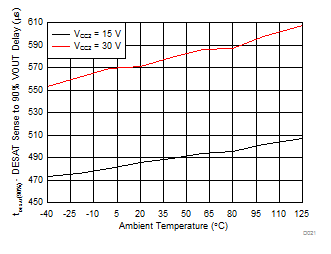
CL = 10 nFRGH = 0 ΩRGL = 0 Ω
Figure 7-34 DESAT Sense to VOUTH/L 90% Delay vs Temperature
GUID-4898F6F1-C421-4869-B74F-4824BB6FC6C1-low.gif
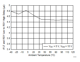
Figure 7-36 Fault and RDY Low to RDY High Delay vs Temperature
GUID-AE207AB3-ADA2-46A1-8E89-4F829ABD642C-low.gif
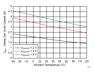
Figure 7-38 Miller Clamp Current vs Temperature
GUID-1F15FEC3-4551-43D6-8314-903C693B303F-low.gif
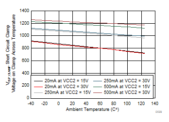
Figure 7-40 VCLP_CLAMP - Short Circuit Clamp Voltage on Clamp Across Temperature
GUID-FD4CA1B2-2810-4BF2-905B-7FBD4902272E-low.gif
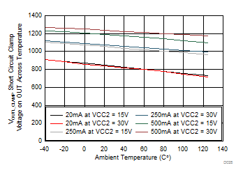
Figure 7-42 VOUTL_CLAMP - Short Circuit Clamp Voltage on OUTL Across Temperature