ZHCSLQ2F january 2020 – february 2023 ISO6720 , ISO6721 , ISO6721R
PRODUCTION DATA
- 1
- 1 特性
- 2 应用
- 3 说明
- 4 Revision History
- 5 Pin Configuration and Functions
-
6 Specifications
- 6.1 Absolute Maximum Ratings
- 6.2 ESD Ratings
- 6.3 Recommended Operating Conditions
- 6.4 Thermal Information
- 6.5 Power Ratings
- 6.6 Insulation Specifications
- 6.7 Safety-Related Certifications
- 6.8 Safety Limiting Values
- 6.9 Electrical Characteristics—5-V Supply
- 6.10 Supply Current Characteristics—5-V Supply
- 6.11 Electrical Characteristics—3.3-V Supply
- 6.12 Supply Current Characteristics—3.3-V Supply
- 6.13 Electrical Characteristics—2.5-V Supply
- 6.14 Supply Current Characteristics—2.5-V Supply
- 6.15 Electrical Characteristics—1.8-V Supply
- 6.16 Supply Current Characteristics—1.8-V Supply
- 6.17 Switching Characteristics—5-V Supply
- 6.18 Switching Characteristics—3.3-V Supply
- 6.19 Switching Characteristics—2.5-V Supply
- 6.20 Switching Characteristics—1.8-V Supply
- 6.21 Insulation Characteristics Curves
- 6.22 Typical Characteristics
- 7 Parameter Measurement Information
- 8 Detailed Description
- 9 Application and Implementation
- 10Power Supply Recommendations
- 11Layout
- 12Device and Documentation Support
- 13Mechanical, Packaging, and Orderable Information
9.2.3 Application Curve
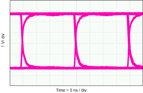
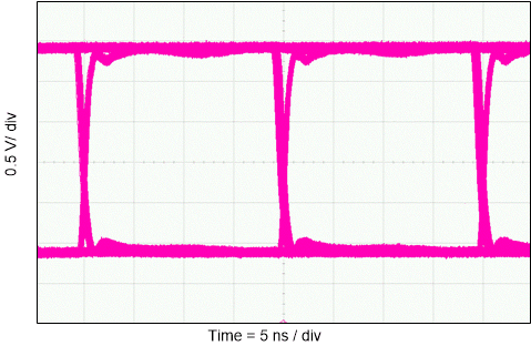
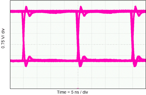
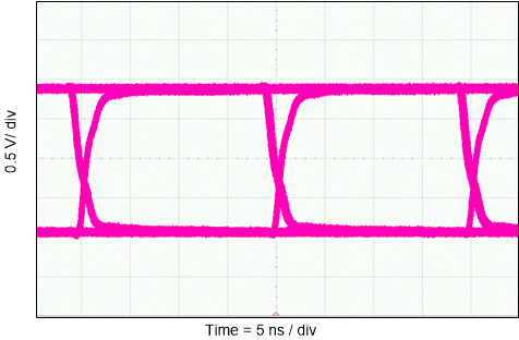
The following typical eye diagrams of the ISO672xB family of devices indicate low jitter and wide open eye at the maximum data rate of 50 Mbps.
 Figure 9-3 Eye Diagram at
50 Mbps PRBS 216 – 1, 5 V and 25°C
 Figure 9-5 Eye Diagram at
50 Mbps PRBS 216 – 1, 2.5 V and 25°C
 Figure 9-4 Eye Diagram at
50 Mbps PRBS 216 – 1, 3.3 V and 25°C
 Figure 9-6 Eye Diagram at
50 Mbps PRBS 216 – 1, 1.8 V and 25°C