ZHCSMP3A December 2019 – June 2021 ISO6731-Q1
PRODUCTION DATA
- 1 特性
- 2 应用
- 3 说明
- 4 Revision History
- 5 Pin Configuration and Functions
-
6 Specifications
- 6.1 Absolute Maximum Ratings
- 6.2 ESD Ratings
- 6.3 Recommended Operating Conditions
- 6.4 Thermal Information
- 6.5 Power Ratings
- 6.6 Insulation Specifications
- 6.7 Safety-Related Certifications
- 6.8 Safety Limiting Values
- 6.9 Electrical Characteristics—5-V Supply
- 6.10 Supply Current Characteristics—5-V Supply
- 6.11 Electrical Characteristics—3.3-V Supply
- 6.12 Supply Current Characteristics—3.3-V Supply
- 6.13 Electrical Characteristics—2.5-V Supply
- 6.14 Supply Current Characteristics—2.5-V Supply
- 6.15 Electrical Characteristics—1.8-V Supply
- 6.16 Supply Current Characteristics—1.8-V Supply
- 6.17 Switching Characteristics—5-V Supply
- 6.18 Switching Characteristics—3.3-V Supply
- 6.19 Switching Characteristics—2.5-V Supply
- 6.20 Switching Characteristics—1.8-V Supply
- 6.21 Insulation Characteristics Curves
- 6.22 Typical Characteristics
- 7 Parameter Measurement Information
- 8 Detailed Description
- 9 Application and Implementation
- 10Power Supply Recommendations
- 11Layout
- 12Device and Documentation Support
- 13Mechanical, Packaging, and Orderable Information
9.2.3 Application Curve
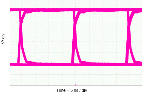
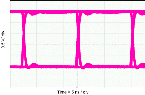
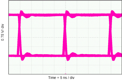
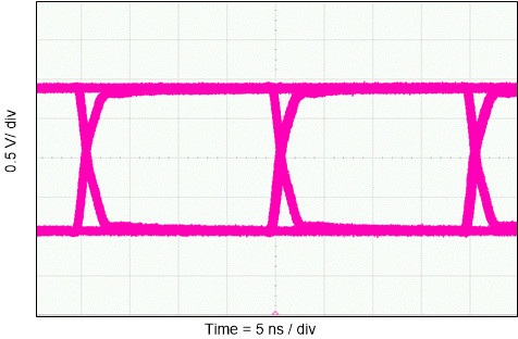
The following typical eye diagrams of the ISO6731-Q1 family of devices indicates low jitter and wide open eye at the maximum data rate of 50 Mbps.
 Figure 9-3 Eye
Diagram at 50 Mbps PRBS 216 – 1, 5 V and 25°C
 Figure 9-5 Eye
Diagram at 50 Mbps PRBS 216 – 1, 2.5 V and 25°C
 Figure 9-4 Eye
Diagram at 50 Mbps PRBS 216 – 1, 3.3 V and 25°C
 Figure 9-6 Eye
Diagram at 50 Mbps PRBS 216 – 1, 1.8 V and 25°C