ZHCSLW8C august 2021 – may 2023 ISO6760-Q1 , ISO6761-Q1 , ISO6762-Q1 , ISO6763-Q1
PRODUCTION DATA
- 1
- 1 特性
- 2 应用
- 3 说明
- 4 Revision History
- 5 Pin Configuration and Functions
-
6 Specifications
- 6.1 Absolute Maximum Ratings
- 6.2 ESD Ratings
- 6.3 Recommended Operating Conditions
- 6.4 Thermal Information
- 6.5 Power Ratings
- 6.6 Insulation Specifications
- 6.7 Safety-Related Certifications
- 6.8 Safety Limiting Values
- 6.9 Electrical Characteristics—5-V Supply
- 6.10 Supply Current Characteristics—5-V Supply
- 6.11 Electrical Characteristics—3.3-V Supply
- 6.12 Supply Current Characteristics—3.3-V Supply
- 6.13 Electrical Characteristics—2.5-V Supply
- 6.14 Supply Current Characteristics—2.5-V Supply
- 6.15 Electrical Characteristics—1.8-V Supply
- 6.16 Supply Current Characteristics—1.8-V Supply
- 6.17 Switching Characteristics—5-V Supply
- 6.18 Switching Characteristics—3.3-V Supply
- 6.19 Switching Characteristics—2.5-V Supply
- 6.20 Switching Characteristics—1.8-V Supply
- 6.21 绝缘特性曲线
- 6.22 Typical Characteristics
- 7 Parameter Measurement Information
- 8 Detailed Description
- 9 Application and Implementation
- 10Power Supply Recommendations
- 11Layout
- 12Device and Documentation Support
- 13Mechanical, Packaging, and Orderable Information
7 Parameter Measurement Information

A. The input pulse is supplied by a generator having the following characteristics: PRR ≤ 50 kHz, 50% duty cycle, tr ≤ 3 ns, tf ≤ 3ns, ZO = 50 Ω. At the input, 50 Ω resistor is required to terminate Input Generator signal. It is not needed in actual application.
B. CL = 15 pF and includes instrumentation and fixture capacitance within ±20%.
Figure 7-1 Switching Characteristics Test Circuit and Voltage Waveforms
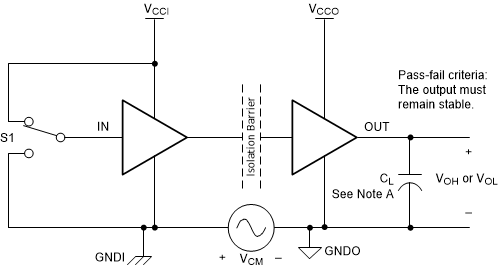
A. CL = 15 pF and includes instrumentation and fixture capacitance within ±20%.
B. Power Supply Ramp Rate = 10 mV/ns
Figure 7-2 Default Output Delay Time Test Circuit and Voltage Waveforms
A. CL = 15 pF and includes instrumentation and fixture capacitance within ±20%.
B. For
optimized CMTI performance, a 0.1 μF + 1 μF decoupling capacitor should be
placed close to VCC1 and VCC2. Please see Section 11.2 for
capacitor placement details. A recommended 0.1μF capacitor is LLL185R71A104MA11L
(CAP CER 0.1UF 10V X7R 0306 - LW Reversed Low ESL Chip Ceramic Capacitors) or
equivalent.
Figure 7-3 Common-Mode Transient Immunity Test Circuit