SLLSE40B September 2010 – November 2024 ISO7240CF-Q1 , ISO7241C-Q1 , ISO7242C-Q1
PRODUCTION DATA
- 1
- 1 Features
- 2 Applications
- 3 Description
- 4 Pin Configurations and Functions
-
5 Specifications
- 5.1 Absolute Maximum Ratings
- 5.2 ESD Ratings
- 5.3 Recommended Operating Conditions
- 5.4 Thermal Characteristics
- 5.5 Power Ratings
- 5.6 Safety-Related Certifications
- 5.7 Safety Limiting Values
- 5.8 Insulation Specifications
- 5.9 Electrical Characteristics: VCC1 and VCC2 at 5-V Operation
- 5.10 Electrical Characteristics: VCC1 and VCC2 at 3.3 V Operation
- 5.11 Electrical Characteristics: VCC1 at 3.3-V, VCC2 at 5-V Operation
- 5.12 Electrical Characteristics: VCC1 at 5-V, VCC2 at 3.3-V Operation
- 5.13 Switching Characteristics: VCC1 and VCC2 at 3.3-V Operation
- 5.14 Switching Characterstics: VCC1 and VCC2 at 5-V Operation
- 5.15 Switching Characteristics: VCC1 at 3.3-V and VCC2 at 5-V Operation
- 5.16 Switching Characteristics: VCC1 at 5-V, VCC2 at 3.3-V Operation
- 5.17 Insulation Characteristics Curves
- 5.18 Typical Characteristic
- 6 Parameter Measurement Information
- 7 Detailed Description
- 8 Application and Implementation
- 9 Device and Documentation Support
- 10Revision History
- 11Mechanical, Packaging, and Orderable Information
5.18 Typical Characteristic
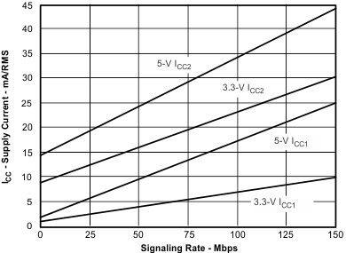 Figure 5-2 ISO7240C RMS Supply Current vs Signaling
Rate
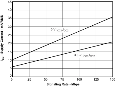 Figure 5-4 ISO7242C RMS Supply Current vs Signaling
Rate
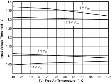 Figure 5-6 Input Voltage Threshold vs Free-Air
Temperature
 Figure 5-8 High-Level Output Current vs High-Level Output
Voltage
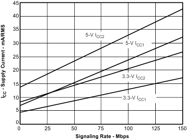 Figure 5-3 ISO7241C RMS Supply Current vs Signaling
Rate
 Figure 5-5 Propogation Delay vs Free-Air
Temperature
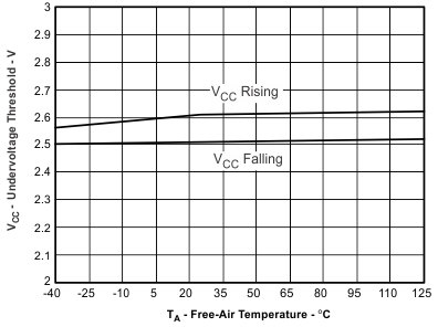 Figure 5-7 VCC1 Failsafe Threshold vs Free-Air
Temperature
 Figure 5-9 Low-Level Output Current vs Low-Level Output
Voltage