SLLSE40B September 2010 – November 2024 ISO7240CF-Q1 , ISO7241C-Q1 , ISO7242C-Q1
PRODUCTION DATA
- 1
- 1 Features
- 2 Applications
- 3 Description
- 4 Pin Configurations and Functions
-
5 Specifications
- 5.1 Absolute Maximum Ratings
- 5.2 ESD Ratings
- 5.3 Recommended Operating Conditions
- 5.4 Thermal Characteristics
- 5.5 Power Ratings
- 5.6 Safety-Related Certifications
- 5.7 Safety Limiting Values
- 5.8 Insulation Specifications
- 5.9 Electrical Characteristics: VCC1 and VCC2 at 5-V Operation
- 5.10 Electrical Characteristics: VCC1 and VCC2 at 3.3 V Operation
- 5.11 Electrical Characteristics: VCC1 at 3.3-V, VCC2 at 5-V Operation
- 5.12 Electrical Characteristics: VCC1 at 5-V, VCC2 at 3.3-V Operation
- 5.13 Switching Characteristics: VCC1 and VCC2 at 3.3-V Operation
- 5.14 Switching Characterstics: VCC1 and VCC2 at 5-V Operation
- 5.15 Switching Characteristics: VCC1 at 3.3-V and VCC2 at 5-V Operation
- 5.16 Switching Characteristics: VCC1 at 5-V, VCC2 at 3.3-V Operation
- 5.17 Insulation Characteristics Curves
- 5.18 Typical Characteristic
- 6 Parameter Measurement Information
- 7 Detailed Description
- 8 Application and Implementation
- 9 Device and Documentation Support
- 10Revision History
- 11Mechanical, Packaging, and Orderable Information
4 Pin Configurations and Functions
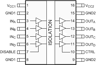
 Figure 4-1 ISO7240CF-Q1 DW
Package16-Pin SOICTop View
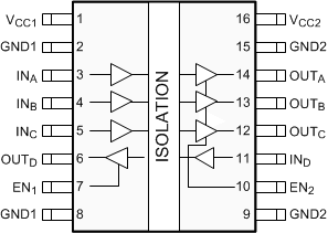
 Figure 4-3 ISO7242C-Q1 DW
Package16-Pin SOICTop View
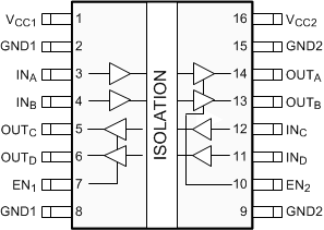
 Figure 4-2 ISO7241C-Q1 DW
Package16-Pin SOICTop View
Figure 4-2 ISO7241C-Q1 DW
Package16-Pin SOICTop ViewTable 4-1 Pin Functions
| PIN | Type(1) | DESCRIPTION | |||
|---|---|---|---|---|---|
| NAME | ISO7240CF-Q1 | ISO7241C-Q1 | ISO7242C-Q1 | ||
| CTRL | 10 | — | — | I | Failsafe output control. Output state is determined by CTRL pin when DISABLE is high or VCC1 is powered down. Output is high when CTRL is high or open and low when CTRL is low. |
| DISABLE | 7 | — | — | I | Input disable. All input pins are disabled when DISABLE is high and enabled when DISABLE is low or open. |
| EN | — | — | — | I | Output enable. All output pins are enabled when EN is high or open and disabled when EN is low. |
| EN1 | — | 7 | 7 | I | Output enable 1. Output pins on side 1 are enabled when EN1 is high or open and disabled when EN1 is low. |
| EN2 | — | 10 | 10 | I | Output enable 2. Output pins on side-2 are enabled when EN2 is high or open and disabled when EN2 is low. |
| GND1 | 2, 8 | 2, 8 | 2, 8 | — | Ground connection for VCC1 |
| GND2 | 9, 15 | 9, 15 | 9, 15 | — | Ground connection for VCC2 |
| INA | 3 | 3 | 3 | I | Input, channel A |
| INB | 4 | 4 | 4 | I | Input, channel B |
| INC | 5 | 5 | 12 | I | Input, channel C |
| IND | 6 | 11 | 11 | I | Input, channel D |
| NC | — | — | — | — | No Connect pins are floating with no internal connection |
| OUTA | 14 | 14 | 14 | O | Output, channel A |
| OUTB | 13 | 13 | 13 | O | Output, channel B |
| OUTC | 12 | 12 | 5 | O | Output, channel C |
| OUTD | 11 | 6 | 6 | O | Output, channel D |
| VCC1 | 1 | 1 | 1 | — | Power supply, VCC1 |
| VCC2 | 16 | 16 | 16 | — | Power supply, VCC2 |
(1) I = Input; O = Output