ZHCSCW1G September 2014 – January 2017 ISO7340C , ISO7340FC , ISO7341C , ISO7341FC , ISO7342C , ISO7342FC
PRODUCTION DATA.
- 1 特性
- 2 应用
- 3 说明
- 4 修订历史记录
- 5 说明 (续)
- 6 Pin Configuration and Functions
-
7 Specifications
- 7.1 Absolute Maximum Ratings
- 7.2 ESD Ratings
- 7.3 Recommended Operating Conditions
- 7.4 Thermal Information
- 7.5 Power Ratings
- 7.6 Insulation Specifications
- 7.7 Safety-Related Certifications
- 7.8 Safety Limiting Values
- 7.9 Electrical Characteristics—5-V Supply
- 7.10 Supply Current Characteristics—5-V Supply
- 7.11 Electrical Characteristics—3.3-V Supply
- 7.12 Supply Current Characteristics—3.3-V Supply
- 7.13 Switching Characteristics—5-V Supply
- 7.14 Switching Characteristics—3.3-V Supply
- 7.15 Insulation Characteristics Curves
- 7.16 Typical Characteristics
- 8 Parameter Measurement Information
- 9 Detailed Description
- 10Application and Implementation
- 11Power Supply Recommendations
- 12Layout
- 13器件和文档支持
- 14机械、封装和可订购信息
7 Specifications
7.1 Absolute Maximum Ratings
See (1)| MIN | MAX | UNIT | |||
|---|---|---|---|---|---|
| VCC | Supply voltage(2) | VCC1, VCC2 | –0.5 | 6 | V |
| Voltage | INx, OUTx, ENx | –0.5 | VCC + 0.5(3) | V | |
| IO | Output current | ±15 | mA | ||
| TJ | Maximum junction temperature | 150 | °C | ||
| Tstg | Storage temperature | –65 | 150 | °C | |
(1) Stresses beyond those listed under absolute maximum ratings may cause permanent damage to the device. These are stress ratings only and functional operation of the device at these or any other conditions beyond those indicated under Recommended Operating Conditions is not implied. Exposure to absolute-maximum-rated conditions for extended periods may affect device reliability.
(2) All voltage values except differential I/O bus voltages are with respect to the local ground terminal (GND1 or GND2) and are peak voltage values.
(3) Maximum voltage must not exceed 6 V.
7.2 ESD Ratings
| VALUE | UNIT | |||
|---|---|---|---|---|
| V(ESD) | Electrostatic discharge | Human body model (HBM), per ANSI/ESDA/JEDEC JS-001(1) | ±4000 | V |
| Charged device model (CDM), per JEDEC specification JESD22-C101(2) | ±1500 | V | ||
(1) JEDEC document JEP155 states that 500-V HBM allows safe manufacturing with a standard ESD control process.
(2) JEDEC document JEP157 states that 250-V CDM allows safe manufacturing with a standard ESD control process.
7.3 Recommended Operating Conditions
| MIN | NOM | MAX | UNIT | ||
|---|---|---|---|---|---|
| VCC1, VCC2 | Supply voltage | 3 | 5.5 | V | |
| IOH | High-level output current | –4 | mA | ||
| IOL | Low-level output current | 4 | mA | ||
| VIH | High-level input voltage | 2 | 5.5 | V | |
| VIL | Low-level input voltage | 0 | 0.8 | V | |
| tui | Input pulse duration | 40 | ns | ||
| 1 / tui | Signaling rate | 0 | 25 | Mbps | |
| TJ | Junction temperature(1) | 136 | °C | ||
| TA | Ambient temperature | –40 | 25 | 125 | °C |
(1) To maintain the recommended operating conditions for TJ, see the Thermal Information table.
7.4 Thermal Information
| THERMAL METRIC(1) | ISO734x | UNIT | ||
|---|---|---|---|---|
| DW (SOIC) | ||||
| 16 PINS | ||||
| RθJA | Junction-to-ambient thermal resistance | 78.4 | °C/W | |
| RθJC(top) | Junction-to-case(top) thermal resistance | 41 | °C/W | |
| RθJB | Junction-to-board thermal resistance | 43 | °C/W | |
| ψJT | Junction-to-top characterization parameter | 15.6 | °C/W | |
| ψJB | Junction-to-board characterization parameter | 42.5 | °C/W | |
| RθJC(bottom) | Junction-to-case(bottom) thermal resistance | n/a | °C/W | |
(1) For more information about traditional and new thermal metrics, see the Semiconductor and IC Package Thermal Metrics application report.
7.5 Power Ratings
VCC1 = VCC2 = 5.5 V, TJ = 150°C, CL = 15 pF, Input a 12.5-MHz 50% duty cycle square wave| PARAMETER | TEST CONDITIONS | MIN | TYP | MAX | UNIT | |
|---|---|---|---|---|---|---|
| PD | Maximum power dissipation by both sides of ISO7340x | 92 | mW | |||
| PD1 | Maximum power dissipation by side-1 of ISO7340x | 24 | ||||
| PD2 | Maximum power dissipation by side-2 of ISO7340x | 68 | ||||
| PD | Maximum power dissipation by both sides of ISO7341x | 102 | mW | |||
| PD1 | Maximum power dissipation by side-1 of ISO7341x | 42 | ||||
| PD2 | Maximum power dissipation by side-2 of ISO7341x | 60 | ||||
| PD | Maximum power dissipation by both sides of ISO7342x | 111 | mW | |||
| PD1 | Maximum power dissipation by side-1 of ISO7342x | 55.5 | ||||
| PD2 | Maximum power dissipation by side-2 of ISO7342x | 55.5 | ||||
7.6 Insulation Specifications
| PARAMETER | TEST CONDITIONS | VALUE | UNIT | |
|---|---|---|---|---|
| GENERAL | ||||
| CLR | External clearance(1) | Shortest terminal-to-terminal distance through air | >8 | mm |
| CPG | External creepage(1) | Shortest terminal-to-terminal distance across the package surface | >8 | mm |
| DTI | Distance through the insulation | Minimum internal gap (internal clearance) | >13 | µm |
| CTI | Comparative tracking index | DIN EN 60112 (VDE 0303-11); IEC 60112 | >400 | V |
| Material group | II | |||
| Overvoltage Category | Rated mains voltage ≤ 300 VRMS | I–IV | ||
| Rated mains voltage ≤ 600 VRMS | I–III | |||
| Rated mains voltage ≤ 1000 VRMS | I-II | |||
| DIN V VDE V 0884-10 (VDE V 0884-10):2006-12(2) | ||||
| VIORM | Maximum repetitive peak isolation voltage | AC voltage (bipolar) | 1414 | VPK |
| VIOTM | Maximum transient isolation voltage | VTEST = VIOTM; t = 60 s (qualification); t = 1 s (100% production) |
4242 | VPK |
| VIOSM | Maximum surge isolation voltage(3) | Test method per IEC 60065, 1.2/50 µs waveform, VTEST = 1.3 × VIOSM = 7800 VPK (qualification) |
6000 | VPK |
| qpd | Apparent charge(4) | Method a: After I/O safety test subgroup 2/3, Vini = VIOTM, tini = 60 s; Vpd(m) = 1.2 × VIORM = 1697 VPK, tm = 10 s |
≤5 | pC |
| Method a: After environmental tests subgroup 1, Vini = VIOTM, tini = 60 s; Vpd(m) = 1.6 × VIORM = 2262 VPK, tm = 10 s |
≤5 | |||
| Method b1: At routine test (100% production) and preconditioning (type test) Vini = VIOTM, tini = 1 s; Vpd(m) = 1.875 × VIORM = 2651 VPK, tm = 1 s (100% production) |
≤5 | |||
| CIO | Barrier capacitance, input to output(5) | VIO = 0.4 sin (2πft), f = 1 MHz | 2.4 | pF |
| RIO | Isolation resistance, input to output(5) | VIO = 500 V, TA = 25°C | >1012 | Ω |
| VIO = 500 V, 100°C ≤ TA ≤ x°C | >1011 | |||
| VIO = 500 V at TS = 150°C | >109 | |||
| Pollution degree | 2 | |||
| Climatic category | 40/125/21 | |||
| UL 1577 | ||||
| VISO | Withstand isolation voltage | VTEST = VISO = 3000 VRMS, t = 60 s (qualification); VTEST = 1.2 × VISO = 3600 VRMS, t = 1 s (100% production) | 3000 | VRMS |
(1) Creepage and clearance requirements should be applied according to the specific equipment isolation standards of an application. Care should be taken to maintain the creepage and clearance distance of a board design to ensure that the mounting pads of the isolator on the printed-circuit board do not reduce this distance. Creepage and clearance on a printed-circuit board become equal in certain cases. Techniques such as inserting grooves and/or ribs on a printed circuit board are used to help increase these specifications.
(2) This coupler is suitable for safe electrical insulation only within the maximum operating ratings. Compliance with the safety ratings shall be ensured by means of suitable protective circuits.
(3) Testing is carried out in air or oil to determine the intrinsic surge immunity of the isolation barrier.
(4) Apparent charge is electrical discharge caused by a partial discharge (pd).
(5) All pins on each side of the barrier tied together creating a two-terminal device
7.7 Safety-Related Certifications
7.8 Safety Limiting Values
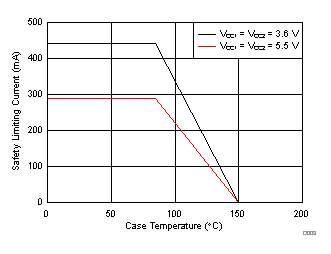
Safety limiting(1) intends to minimize potential damage to the isolation barrier upon failure of input or output circuitry. A failure of the I/O can allow low resistance to ground or the supply and, without current limiting, dissipate sufficient power to overheat the die and damage the isolation barrier, potentially leading to secondary system failures.| PARAMETER | TEST CONDITIONS | MIN | TYP | MAX | UNIT | |
|---|---|---|---|---|---|---|
| IS | Safety input, output, or supply current | RθJA = 78.4 °C/W, VI = 5.5 V, TJ = 150°C, TA = 25°C, see Figure 1 | 290 | mA | ||
| RθJA = 78.4 °C/W, VI = 3.6 V, TJ = 150°C, TA = 25°C, see Figure 1 | 443 | |||||
| TS | Safety temperature | 150 | ||||
(1) The safety-limiting constraint is the maximum junction temperature specified in the data sheet. The power dissipation and junction-to-air thermal impedance of the device installed in the application hardware determines the junction temperature. The assumed junction-to-air thermal resistance in the Thermal Information table is that of a device installed on a high-K test board for leaded surface-mount packages. The power is the recommended maximum input voltage times the current. The junction temperature is then the ambient temperature plus the power times the junction-to-air thermal resistance.
7.9 Electrical Characteristics—5-V Supply
VCC1 and VCC2 at 5 V ± 10% (over recommended operating conditions unless otherwise noted)| PARAMETER | TEST CONDITIONS | MIN | TYP | MAX | UNIT | |
|---|---|---|---|---|---|---|
| VOH | High-level output voltage | IOH = –4 mA; see Figure 14 | VCCO(1) – 0.5 | 4.7 | V | |
| IOH = –20 μA; see Figure 14 | VCCO(1) – 0.1 | 5 | ||||
| VOL | Low-level output voltage | IOL = 4 mA; see Figure 14 | 0.2 | 0.4 | V | |
| IOL = 20 μA; see Figure 14 | 0 | 0.1 | ||||
| VI(HYS) | Input threshold voltage hysteresis | 480 | mV | |||
| IIH | High-level input current | VIH = VCC at INx or ENx | 10 | μA | ||
| IIL | Low-level input current | VIL = 0 V at INx or ENx | –10 | μA | ||
| CMTI | Common-mode transient immunity | VI = VCC or 0 V; see Figure 17 | 25 | 70 | kV/μs | |
| CI | Input capacitance(2) | VI = VCC/2 + 0.4 sin (2πft), f = 1 MHz, VCC = 5 V | 3.4 | pF | ||
(1) VCCO is supply voltage, VCC1 or VCC2, for the output channel being measured.
(2) Measured from input pin to ground.
7.10 Supply Current Characteristics—5-V Supply
All inputs switching with square wave clock signal for dynamic ICC measurement. VCC1 and VCC2 at 5 V ± 10% (over recommended operating conditions unless otherwise noted)7.11 Electrical Characteristics—3.3-V Supply
VCC1 and VCC2 at 3.3 V ± 10% (over recommended operating conditions unless otherwise noted)| PARAMETER | TEST CONDITIONS | MIN | TYP | MAX | UNIT | |
|---|---|---|---|---|---|---|
| VOH | High-level output voltage | IOH = –4 mA; see Figure 14 | VCCO(1) – 0.5 | 3 | V | |
| IOH = –20 μA; see Figure 14 | VCCO(1) – 0.1 | 3.3 | ||||
| VOL | Low-level output voltage | IOL = 4 mA; see Figure 14 | 0.2 | 0.4 | V | |
| IOL = 20 μA; see Figure 14 | 0 | 0.1 | ||||
| VI(HYS) | Input threshold voltage hysteresis | 450 | mV | |||
| IIH | High-level input current | VIH = VCC at INx or ENx | 10 | μA | ||
| IIL | Low-level input current | VIL = 0 V at INx or ENx | –10 | μA | ||
| CMTI | Common-mode transient immunity | VI = VCC or 0 V; see Figure 17 | 25 | 50 | kV/μs | |
(1) VCCO is supply voltage, VCC1 or VCC2, for the output channel being measured.
7.12 Supply Current Characteristics—3.3-V Supply
All inputs switching with square wave clock signal for dynamic ICC measurement. VCC1 and VCC2 at 3.3 V ± 10% (over recommended operating conditions unless otherwise noted)7.13 Switching Characteristics—5-V Supply
VCC1 and VCC2 at 5 V ± 10% (over recommended operating conditions unless otherwise noted)| PARAMETER | TEST CONDITIONS | MIN | TYP | MAX | UNIT | ||
|---|---|---|---|---|---|---|---|
| tPLH, tPHL | Propagation delay time | See Figure 14 | 20 | 31 | 58 | ns | |
| PWD(1) | Pulse width distortion |tPHL – tPLH| | 4 | ns | ||||
| tsk(o)(2) | Channel-to-channel output skew time | Same-direction Channels | 2.5 | ns | |||
| Opposite-direction Channels | 17 | ns | |||||
| tsk(pp)(3) | Part-to-part skew time | 23 | ns | ||||
| tr | Output signal rise time | See Figure 14 | 2.1 | ns | |||
| tf | Output signal fall time | 1.7 | ns | ||||
| tPHZ | Disable propagation delay, high-to-high impedance output | See Figure 15 | 7 | 13 | ns | ||
| tPLZ | Disable propagation delay, low-to-high impedance output | 7 | 13 | ns | |||
| tPZH | Enable propagation delay, high impedance-to-high output | ISO734xC | 7 | 13 | ns | ||
| ISO734xFC | 15000 | 23000(4) | |||||
| tPZL | Enable propagation delay, high impedance-to-low output | ISO734xC | 15000 | 23000(4) | ns | ||
| ISO734xFC | 7 | 13 | |||||
| tfs | Fail-safe output delay time from input power loss | See Figure 16 | 9.4 | μs | |||
(1) Also known as Pulse Skew.
(2) tsk(o) is the skew between outputs of a single device with all driving inputs connected together and the outputs switching in the same direction while driving identical loads.
(3) tsk(pp) is the magnitude of the difference in propagation delay times between any terminals of different devices switching in the same direction while operating at identical supply voltages, temperature, input signals and loads.
(4) The enable signal rate should be ≤ 43 Kbps.
7.14 Switching Characteristics—3.3-V Supply
VCC1 and VCC2 at 3.3 V ± 10% (over recommended operating conditions unless otherwise noted)| PARAMETER | TEST CONDITIONS | MIN | TYP | MAX | UNIT | ||
|---|---|---|---|---|---|---|---|
| tPLH, tPHL | Propagation delay time | See Figure 14 | 22 | 35 | 66 | ns | |
| PWD(1) | Pulse width distortion |tPHL – tPLH| | 2.5 | |||||
| tsk(o) (2) | Channel-to-channel output skew time | Same-direction Channels | 3 | ||||
| Opposite-direction Channels | 16 | ||||||
| tsk(pp) (3) | Part-to-part skew time | 28 | |||||
| tr | Output signal rise time | See Figure 14 | 2.8 | ns | |||
| tf | Output signal fall time | 2.1 | |||||
| tPHZ | Disable propagation delay, high-to-high impedance output | See Figure 15 | 9 | 18 | ns | ||
| tPLZ | Disable propagation delay, low-to-high impedance output | 9 | 18 | ||||
| tPZH | Enable propagation delay, high impedance-to-high output | ISO734xC | 9 | 18 | |||
| ISO734xFC | 16000 | 24000(4) | |||||
| tPZL | Enable propagation delay, high impedance-to-low output | ISO734xC | 16000 | 24000(4) | |||
| ISO734xFC | 9 | 18 | |||||
| tfs | Fail-safe output delay time from input power loss | See Figure 16 | 9.4 | μs | |||
(1) Also known as Pulse Skew.
(2) tsk(o) is the skew between outputs of a single device with all driving inputs connected together and the outputs switching in the same direction while driving identical loads.
(3) tsk(pp) is the magnitude of the difference in propagation delay times between any terminals of different devices switching in the same direction while operating at identical supply voltages, temperature, input signals and loads.
(4) The enable signal rate should be ≤ 45 Kbps.
7.15 Insulation Characteristics Curves
7.16 Typical Characteristics
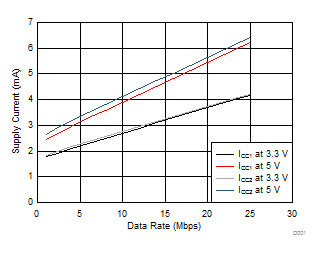
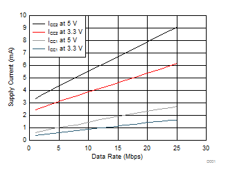
| TA = 25°C | CL = 15 pF |
(15-pF Load)
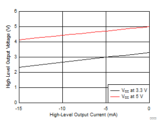
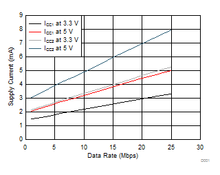
| TA = 25°C |
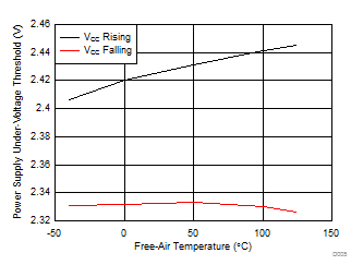
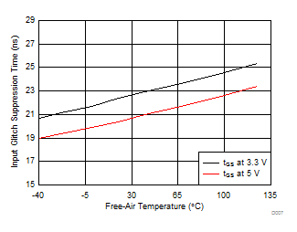
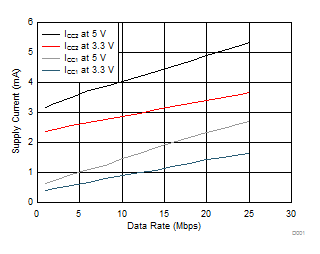
| TA = 25°C | CL = No Load |
(No Load)
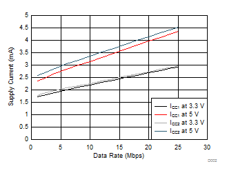
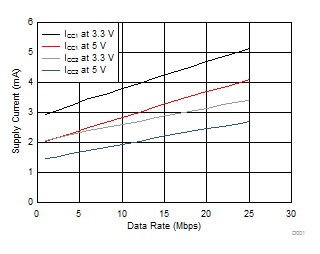
| TA = 25°C | CL = No Load |
(No Load)
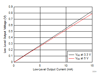
| TA = 25°C |
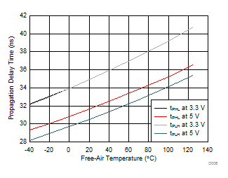
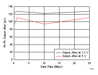
| TA = 25°C |
