ZHCSCW1G September 2014 – January 2017 ISO7340C , ISO7340FC , ISO7341C , ISO7341FC , ISO7342C , ISO7342FC
PRODUCTION DATA.
- 1 特性
- 2 应用
- 3 说明
- 4 修订历史记录
- 5 说明 (续)
- 6 Pin Configuration and Functions
-
7 Specifications
- 7.1 Absolute Maximum Ratings
- 7.2 ESD Ratings
- 7.3 Recommended Operating Conditions
- 7.4 Thermal Information
- 7.5 Power Ratings
- 7.6 Insulation Specifications
- 7.7 Safety-Related Certifications
- 7.8 Safety Limiting Values
- 7.9 Electrical Characteristics—5-V Supply
- 7.10 Supply Current Characteristics—5-V Supply
- 7.11 Electrical Characteristics—3.3-V Supply
- 7.12 Supply Current Characteristics—3.3-V Supply
- 7.13 Switching Characteristics—5-V Supply
- 7.14 Switching Characteristics—3.3-V Supply
- 7.15 Insulation Characteristics Curves
- 7.16 Typical Characteristics
- 8 Parameter Measurement Information
- 9 Detailed Description
- 10Application and Implementation
- 11Power Supply Recommendations
- 12Layout
- 13器件和文档支持
- 14机械、封装和可订购信息
9 Detailed Description
9.1 Overview
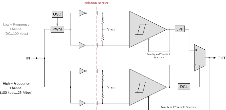
The isolator in Figure 18 is based on a capacitive isolation-barrier technique. The I/O channel of the device consists of two internal data channels, a high-frequency (HF) channel with a bandwidth from 100 kbps up to 25 Mbps, and a low-frequency (LF) channel covering the range from 100 kbps down to DC.
In principle, a single-ended input signal entering the HF channel is split into a differential signal through the inverter gate at the input. The following capacitor-resistor networks differentiate the signal into transient pulses, which then are converted into CMOS levels by a comparator. The transient pulses at the input of the comparator can be either above or below the common-mode voltage VREF depending on whether the input bit transitioned from 0 to 1 or 1 to 0. The comparator threshold is adjusted based on the expected bit transition. A decision logic (DCL) at the output of the HF channel comparator measures the durations between signal transients. If the duration between two consecutive transients exceeds a certain time limit, (as in the case of a low-frequency signal), the DCL forces the output-multiplexer to switch from the high-frequency to the low-frequency channel.
Because low-frequency input signals require the internal capacitors to assume prohibitively large values, these signals are pulse-width modulated (PWM) with the carrier frequency of an internal oscillator, thus creating a sufficiently high frequency, capable of passing the capacitive barrier. As the input is modulated, a low-pass filter (LPF) is needed to remove the high-frequency carrier from the actual data before passing it on to the output multiplexer.
9.2 Functional Block Diagram
 Figure 18. Conceptual Block Diagram of a Digital Capacitive Isolator
9.3 Feature Description
The ISO734x family of devices are available in multiple channel configurations and default output state options to enable wide variety of application uses.
| PART NUMBER | CHANNEL DIRECTION | RATED ISOLATION | MAXIMUM DATA RATE | DEFAULT OUTPUT |
|---|---|---|---|---|
| ISO7340C | 4 Forward, 0 Reverse |
3000 VRMS / 4242 VPK(1) | 25 Mbps | High |
| ISO7340FC | Low | |||
| ISO7341C | 3 Forward, 1 Reverse |
High | ||
| ISO7341FC | Low | |||
| ISO7342C | 2 Forward, 2 Reverse |
High | ||
| ISO7342FC | Low |
9.3.1 Electromagnetic Compatibility (EMC) Considerations
Many applications in harsh industrial environment are sensitive to disturbances such as electrostatic discharge (ESD), electrical fast transient (EFT), surge, and electromagnetic emissions. These electromagnetic disturbances are regulated by international standards such as IEC 61000-4-x and CISPR 22. Although system-level performance and reliability depends, to a large extent, on the application board design and layout, the ISO734x family of devices incorporates many chip-level design improvements for overall system robustness. Some of these improvements include:
- Robust ESD protection cells for input and output signal pins and inter-chip bond pads.
- Low-resistance connectivity of ESD cells to supply and ground pins.
- Enhanced performance of high voltage isolation capacitor for better tolerance of ESD, EFT and surge events.
- Bigger on-chip decoupling capacitors to bypass undesirable high energy signals through a low impedance path.
- PMOS and NMOS devices isolated from each other by using guard rings to avoid triggering of parasitic SCRs.
- Reduced common mode currents across the isolation barrier by ensuring purely differential internal operation.
9.4 Device Functional Modes
Table 1 lists the functional modes for the ISO734x family of devices.
Table 1. Function Table(1)
| VCCI | VCCO | INPUT (INx) |
OUTPUT ENABLE (ENx) |
OUTPUT (OUTx) |
|
|---|---|---|---|---|---|
| ISO734xC | ISO734xFC | ||||
| PU | PU | H | H or Open | H | H |
| L | H or Open | L | L | ||
| X | L | Z | Z | ||
| Open | H or Open | H(2) | L(3) | ||
| PD | PU | X | H or Open | H(2) | L(3) |
| X | PU | X | L | Z | Z |
| X | PD | X | X | Undetermined | Undetermined |
