SLLS984I June   2009  – July 2015 ISO7420 , ISO7420M , ISO7421

UNLESS OTHERWISE NOTED, this document contains PRODUCTION DATA.  

  1. Features
  2. Applications
  3. Description
  4. Revision History
  5. Pin Configuration and Functions
  6. Specifications
    1. 6.1  Absolute Maximum Ratings
    2. 6.2  ESD Ratings
    3. 6.3  Recommended Operating Conditions
    4. 6.4  Thermal Information
    5. 6.5  Electrical Characteristics: VCC1 and VCC2 at 5 V ±5%
    6. 6.6  Electrical Characteristics: VCC1 at 5 V ±5%, VCC2 at 3.3 V ±5%
    7. 6.7  Electrical Characteristics: VCC1 at 3.3 V ±5%, VCC2 at 5 V ±5%
    8. 6.8  Electrical Characteristics: VCC1 and VCC2 at 3.3 V ±5%
    9. 6.9  Power Dissipation Characteristics
    10. 6.10 Switching Characteristics: VCC1 and VCC2 at 5 V ±5%
    11. 6.11 Switching Characteristics: VCC1 at 5 V ±5%, VCC2 at 3.3 V ±5%
    12. 6.12 Switching Characteristics: VCC1 at 3.3 V ±5%, VCC2 at 5 V ±5%
    13. 6.13 Switching Characteristics: VCC1 and VCC2 at 3.3 V ±5%
    14. 6.14 Typical Characteristics
  7. Parameter Measurement Information
  8. Detailed Description
    1. 8.1 Overview
    2. 8.2 Functional Block Diagram
    3. 8.3 Feature Description
      1. 8.3.1 Insulation Characteristics
      2. 8.3.2 Package Characteristics
      3. 8.3.3 Safety Limiting Values
      4. 8.3.4 Regulatory Information
    4. 8.4 Device Functional Modes
      1. 8.4.1 Device I/O Schematics
  9. Application and Implementation
    1. 9.1 Application Information
    2. 9.2 Typical Application
      1. 9.2.1 Design Requirements
      2. 9.2.2 Detailed Design Procedure
      3. 9.2.3 Application Curve
  10. 10Power Supply Recommendations
  11. 11Layout
    1. 11.1 Layout Guidelines
      1. 11.1.1 PCB Material
    2. 11.2 Layout Example
  12. 12Device and Documentation Support
    1. 12.1 Documentation Support
      1. 12.1.1 Related Documentation
    2. 12.2 Related Links
    3. 12.3 Community Resources
    4. 12.4 Trademarks
    5. 12.5 Electrostatic Discharge Caution
    6. 12.6 Glossary
  13. 13Mechanical, Packaging, and Orderable Information

封装选项

机械数据 (封装 | 引脚)
散热焊盘机械数据 (封装 | 引脚)
订购信息

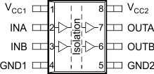
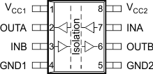
5 Pin Configuration and Functions

ISO7420: D Package
8-Pin SOIC
(Top View)
ISO7420 ISO7420M ISO7421 po_iso7420_lls984.gif
ISO7421: D Package
8-Pin SOIC
(Top View)
ISO7420 ISO7420M ISO7421 po_iso7421_lls984.gif

Pin Functions

PIN I/O DESCRIPTION
NAME ISO7420 ISO7421
GND1 4 4 Ground connection for VCC1
GND2 5 5 Ground connection for VCC2
INA 2 7 I Input, channel A
INB 3 3 I Input, channel B
OUTA 7 2 O Output, channel A
OUTB 6 6 O Output, channel B
VCC1 1 1 Power supply, VCC1
VCC2 8 8 Power supply, VCC2