ZHCS349G September 2011 – January 2015 ISO7640FM , ISO7641FM
UNLESS OTHERWISE NOTED, this document contains PRODUCTION DATA.
- 1 特性
- 2 应用
- 3 说明
- 4 修订历史记录
- 5 Pin Configuration and Functions
-
6 Specifications
- 6.1 Absolute Maximum Ratings
- 6.2 ESD Ratings
- 6.3 Recommended Operating Conditions
- 6.4 Thermal Information
- 6.5 Electrical Characteristics: VCC1 and VCC2 at 5 V ±10%
- 6.6 Electrical Characteristics: VCC1 at 5 V ±10% and VCC2 at 3.3 V ±10%
- 6.7 Electrical Characteristics: VCC1 at 3.3 V ±10% and VCC2 at 5 V ±10%
- 6.8 Electrical Characteristics: VCC1 and VCC2 at 3.3 V ±10%
- 6.9 Electrical Characteristics: VCC1 and VCC2 at 2.7 V
- 6.10 Supply Current: VCC1 and VCC2 at 5 V ±10%
- 6.11 Supply Current: VCC1 at 5 V ±10% and VCC2 at 3.3 V ±10%
- 6.12 Supply Current: VCC1 at 3.3 V ±10% and VCC2 at 5 V ±10%
- 6.13 Supply Current: VCC1 and VCC2 at 3.3 V ±10%
- 6.14 Supply Current: VCC1 and VCC2 at 2.7 V
- 6.15 Switching Characteristics: VCC1 and VCC2 at 5 V ±10%
- 6.16 Switching Characteristics: VCC1 at 5 V ±10% and VCC2 at 3.3 V ±10%
- 6.17 Switching Characteristics: VCC1 at 3.3 V ±10% and VCC2 at 5 V ±10%
- 6.18 Switching Characteristics: VCC1 and VCC2 at 3.3 V ±10%
- 6.19 Switching Characteristics: VCC1 and VCC2 at 2.7 V
- 6.20 Typical Characteristics
- 7 Parameter Measurement Information
- 8 Detailed Description
- 9 Application and Implementation
- 10Power Supply Recommendations
- 11Layout
- 12器件和文档支持
- 13机械封装和可订购信息
7 Parameter Measurement Information

A. The input pulse is supplied by a generator having the following characteristics: PRR ≤ 50 kHz, 50% duty cycle, tr ≤ 3 ns, tf ≤ 3ns, ZO = 50 Ω. At the input, 50-Ω resistor is required to terminate Input Generator signal. It is not needed in actual application.
B. CL = 15 pF and includes instrumentation and fixture capacitance within ±20%.
Figure 9. Switching Characteristics Test Circuit and Voltage Waveforms

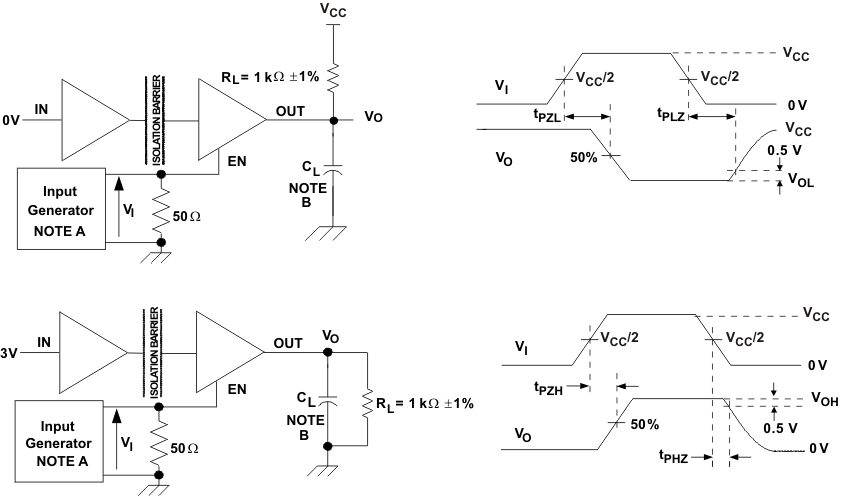
A. The input pulse is supplied by a generator having the following characteristics: PRR ≤ 10 kHz, 50% duty cycle,
tr ≤ 3 ns, tf ≤ 3 ns, ZO = 50 Ω.
tr ≤ 3 ns, tf ≤ 3 ns, ZO = 50 Ω.
B. CL = 15 pF and includes instrumentation and fixture capacitance within ±20%.
Figure 10. Enable/Disable Propagation Delay Time Test Circuit and Waveform

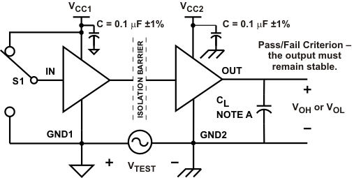
A. CL = 15 pF and includes instrumentation and fixture capacitance within ±20%.
Figure 11. Fail-Safe Delay Time Test Circuit and Voltage Waveforms
