ZHCSE61A July 2015 – September 2015 ISO7830
PRODUCTION DATA.
- 1 特性
- 2 应用范围
- 3 说明
- 4 修订历史记录
- 5 Pin Configuration and Functions
-
6 Specifications
- 6.1 Absolute Maximum Ratings
- 6.2 ESD Ratings
- 6.3 Recommended Operating Conditions
- 6.4 Thermal Information
- 6.5 Power Rating
- 6.6 Electrical Characteristics, 5 V
- 6.7 Electrical Characteristics, 3.3 V
- 6.8 Electrical Characteristics, 2.5 V
- 6.9 Switching Characteristics, 5 V
- 6.10 Switching Characteristics, 3.3 V
- 6.11 Switching Characteristics, 2.5 V
- 6.12 Typical Characteristics
- 7 Parameter Measurement Information
- 8 Detailed Description
- 9 Application and Implementation
- 10Power Supply Recommendations
- 11Layout
- 12器件和文档支持
- 13机械、封装和可订购信息
封装选项
请参考 PDF 数据表获取器件具体的封装图。
机械数据 (封装 | 引脚)
- DWW|16
- DW|16
散热焊盘机械数据 (封装 | 引脚)
订购信息
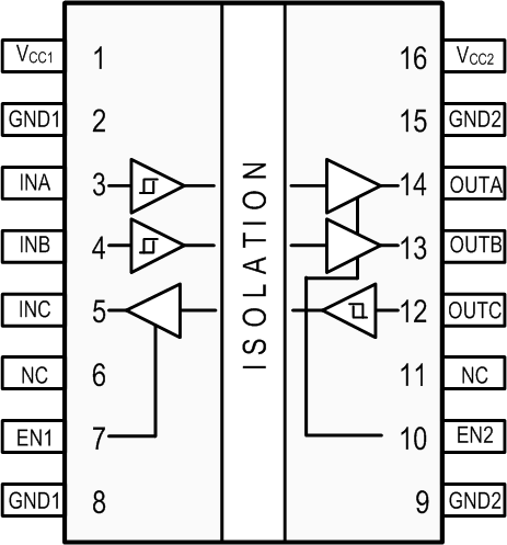
5 Pin Configuration and Functions
DW Package
16-Pin SOIC
Top View

Pin Functions
| PIN | I/O | DESCRIPTION | |
|---|---|---|---|
| NAME | NO. | ||
| EN1 | 7 | I | Output enable 1. Output pins on side 1 are enabled when EN1 is high or open and in high-impedance state when EN1 is low. |
| EN2 | 10 | I | Output enable 2. Output pins on side 2 are enabled when EN2 is high or open and in high-impedance state when EN2 is low. |
| GND1 | 2, 8 | — | Ground connection for VCC1 |
| GND2 | 9, 15 | — | Ground connection for VCC2 |
| INA | 3 | I | Input, channel A |
| INB | 4 | I | Input, channel B |
| INC | 5 | I | Input, channel C |
| OUTA | 14 | O | Output, channel A |
| OUTB | 13 | O | Output, channel B |
| OUTC | 12 | O | Output, channel C |
| NC | 6, 11 | — | Not connected |
| VCC1 | 1 | — | Power supply, VCC1 |
| VCC2 | 16 | — | Power supply, VCC2 |