ZHCSHP9C May 2017 – October 2018 IWR1443
PRODUCTION DATA.
- 1器件概述
- 2修订历史记录
- 3Device Comparison
- 4Terminal Configuration and Functions
-
5Specifications
- 5.1 Absolute Maximum Ratings
- 5.2 ESD Ratings
- 5.3 Power-On Hours (POH)
- 5.4 Recommended Operating Conditions
- 5.5 Power Supply Specifications
- 5.6 Power Consumption Summary
- 5.7 RF Specification
- 5.8 Thermal Resistance Characteristics for FCBGA Package [ABL0161]
- 5.9
Timing and Switching Characteristics
- 5.9.1 Power Supply Sequencing and Reset Timing
- 5.9.2 Synchronized Frame Triggering
- 5.9.3 Input Clocks and Oscillators
- 5.9.4 Multibuffered / Standard Serial Peripheral Interface (MibSPI)
- 5.9.5 LVDS Interface Configuration
- 5.9.6 General-Purpose Input/Output
- 5.9.7 Controller Area Network Interface (DCAN)
- 5.9.8 Serial Communication Interface (SCI)
- 5.9.9 Inter-Integrated Circuit Interface (I2C)
- 5.9.10 Quad Serial Peripheral Interface (QSPI)
- 5.9.11 JTAG Interface
- 5.9.12 Camera Serial Interface (CSI)
- 6Detailed Description
- 7Applications, Implementation, and Layout
- 8Device and Documentation Support
- 9Mechanical, Packaging, and Orderable Information
Table 5-23 CSI Switching Characteristics
over operating Tj temperature range (unless otherwise noted)| PARAMETER | MIN | TYP | MAX | UNIT | ||
|---|---|---|---|---|---|---|
| HPTX | ||||||
| HSTXDBR | Data bit rate | (1 or 2 data lane PHY) | 150 | 600 | Mbps | |
| (4 data lane PHY) | 150 | 600 | ||||
| fCLK | DDR clock frequency | (1 or 2 data lane PHY) | 75 | 450 | MHz | |
| (4 data lane PHY) | 75 | 300 | ||||
| ΔVCMTX(LF) | Common-level variation from 75 to 450 MHz of CSI2 clock frequency | –50 | 50 | mVpeak | ||
| tR and tF | 20% to 80% rise time and fall time | 150 | ns | |||
| 0.3 | UI | |||||
| LPTX DRIVER | ||||||
| tRLP and tFLP | 15% to 85% rise time and fall time | 25 | ns | |||
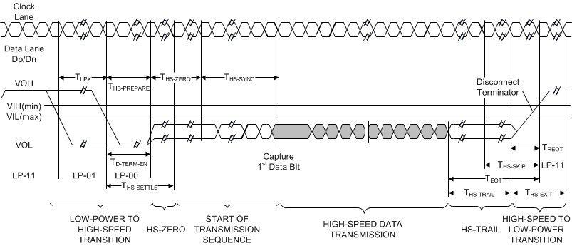
| tEOT(1) | Time from start of THS-TRAIL period to start of LP-11 state | 105 + 12*UI | ns | |||
| δV/δtSR(2)(3)(4) | Slew rate. CLOAD = 0 to 5 pF | 500 | mV/ns | |||
| Slew rate. CLOAD = 5 to 20 pF | 200 | |||||
| Slew rate. CLOAD = 20 to 70 pF | 100 | |||||
| CLOAD(2) | Load capacitance | 0 | 70 | pF | ||
| DATA-CLOCK Timing Specification | ||||||
| UINOM | Nominal Unit Interval (1, 2, or 3 data lane PHY) | 1.11 | 13.33 | ns | ||
| Nominal Unit Interval (4 data lane PHY) | 1.67 | 13.33 | ||||
| UIINST,MIN | Minimum instantaneous Unit Interval (1, 2, or 3 data lane PHY) | 1.033 | 0.975*UINOM – 0.05 | ns | ||
| Minimum instantaneous Unit Interval (4 data lane PHY) | 1.131 | |||||
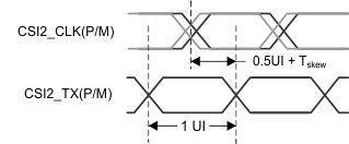
| TSKEW[TX] | Data to clock skew measured at transmitter | –0.15 | 0.15 | UIINST,MIN | ||
| CSI2 TIMING SPECIFICATION | ||||||
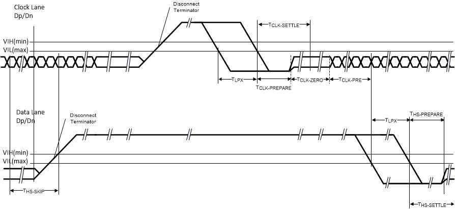
| TCLK-MISS | Time-out for receiver to detect absence of clock transitions and disable the clock lane HS-RX. | 60 | ns | |||
| TCLK-POST | Time that the transmitter continues to send HS clock after the last associated data lane has transitioned to lp mode. Interval is defined as the period from the end of THS-TRAIL to the beginning of TCLK-TRAIL. | 60 ns + 52*UI | ns | |||
| TCLK-PRE | Time that the HS clock shall be driven by the transmitter before any associated data lane beginning the transition from LP to HS mode. | 8 | ns | |||
| TCLK-PREPARE | Time that the transmitter drives the clock lane LP-00 line state immediately before the HS-0 line state starting the HS transmission. | 38 | 95 | ns | ||
| TCLK-TERM-EN | Time for the clock lane receiver to enable the HS line termination, starting from the time point when Dn crosses VIL,MAX. | Time for Dn to reach VTERM-EN | 38 | ns | ||
| TCLK-TRAIL | Time that the transmitter drives the HS-0 state after the last payload clock bit of a HS transmission burst. | 60 | ns | |||
| TCLK-PREPARE + TCLK-ZERO | TCLK-PREPARE + time that the transmitter drives the HS-0 state before starting the clock. | 300 | ns | |||
| TD-TERM-EN | Time for the data lane receiver to enable the HS line termination, starting from the time point when Dn crosses VIL,MAX. | Time for Dn to reach VTERM-EN | 35 ns + 4*UI | ns | ||
| TEOT | Transmitted time interval from the start of THS-TRAIL or TCLKTRAIL, to the start of the LP-11 state following a HS burst. | 105 ns + n*12*UI | ns | |||
| THS-PREPARE | Time that the transmitter drives the data lane LP-00 line state immediately before the HS-0 line state starting the HS transmission | 40 + 4*UI | 85 + 6*UI | ns | ||
| THS-PREPARE + THS-ZERO | THS-PREPARE + time that the transmitter drives the HS-0 state prior to transmitting the Sync sequence. | 145 ns + 10*UI | ns | |||
| THS-SKIP | Time interval during which the HS-RX should ignore any transitions on the data lane, following a HS burst. The end point of the interval is defined as the beginning of the LP-11 state following the HS burst. | 40 | 55 ns + 4*UI | ns | ||
| THS-EXIT | Time that the transmitter drives LP-11 following a HS burst. | 100 | ns | |||
| THS-TRAIL | Time that the transmitter drives the flipped differential state after last payload data bit of a HS transmission burst | max(n*8*UI, 60 ns + n*4*UI)(5)(6) | ns | |||
| TLPX | Transmitted length of any low-power state period | 50(7) | ns | |||
(1) With an additional load capacitance CCM of 0 to 60 pF on the termination center tap at RX side of the lane
(2) While driving CLOAD. Load capacitance includes 50 pF of transmission line capacitance, and 10 pF each for TX and RX.
(3) When the output voltage is from 15% to 85% of the fully settled LP signal levels
(4) Measured as average across any 50 mV segment of the output signal transition
(5) If a > b then max(a, b) = a, otherwise max(a, b) = b.
(6) Where n = 1 for Forward-direction HS mode and n = 4 for Reverse-direction HS mode
(7) TLPX is an internal state machine timing reference. Externally measured values may differ slightly from the specified values due to asymmetrical rise and fall times.
 Figure 5-18 Clock and Data Timing in HS Transmission
  Figure 5-19 High-Speed Data Transmission Burst
1. The HS to LP transition of the CLK does not actually take place since the CLK is always ON in HS mode.
Figure 5-20 Switching the Clock Lane Between Clock Transmission and Low-Power Mode