ZHCSHP9C May   2017  – October 2018 IWR1443

PRODUCTION DATA.  

  1. 1器件概述
    1. 1.1 特性
    2. 1.2 应用
    3. 1.3 说明
    4. 1.4 功能框图
  2. 2修订历史记录
  3. 3Device Comparison
    1. 3.1 Related Products
  4. 4Terminal Configuration and Functions
    1. 4.1 Pin Diagram
    2. 4.2 Signal Descriptions
      1. Table 4-1 Signal Descriptions
    3. 4.3 Pin Multiplexing
  5. 5Specifications
    1. 5.1 Absolute Maximum Ratings
    2. 5.2 ESD Ratings
    3. 5.3 Power-On Hours (POH)
    4. 5.4 Recommended Operating Conditions
    5. 5.5 Power Supply Specifications
    6. 5.6 Power Consumption Summary
    7. 5.7 RF Specification
    8. 5.8 Thermal Resistance Characteristics for FCBGA Package [ABL0161]
    9. 5.9 Timing and Switching Characteristics
      1. 5.9.1  Power Supply Sequencing and Reset Timing
      2. 5.9.2  Synchronized Frame Triggering
      3. 5.9.3  Input Clocks and Oscillators
        1. 5.9.3.1 Clock Specifications
      4. 5.9.4  Multibuffered / Standard Serial Peripheral Interface (MibSPI)
        1. 5.9.4.1 Peripheral Description
        2. 5.9.4.2 MibSPI Transmit and Receive RAM Organization
          1. Table 5-8  SPI Timing Conditions
          2. Table 5-9  SPI Master Mode Switching Parameters (CLOCK PHASE = 0, SPICLK = output, SPISIMO = output, and SPISOMI = input)
          3. Table 5-10 SPI Master Mode Switching Parameters (CLOCK PHASE = 1, SPICLK = output, SPISIMO = output, and SPISOMI = input)
        3. 5.9.4.3 SPI Slave Mode I/O Timings
          1. Table 5-11 SPI Slave Mode Switching Parameters (SPICLK = input, SPISIMO = input, and SPISOMI = output)
        4. 5.9.4.4 Typical Interface Protocol Diagram (Slave Mode)
      5. 5.9.5  LVDS Interface Configuration
        1. 5.9.5.1 LVDS Interface Timings
      6. 5.9.6  General-Purpose Input/Output
        1. Table 5-13 Switching Characteristics for Output Timing versus Load Capacitance (CL)
      7. 5.9.7  Controller Area Network Interface (DCAN)
        1. Table 5-14 Dynamic Characteristics for the DCANx TX and RX Pins
      8. 5.9.8  Serial Communication Interface (SCI)
        1. Table 5-15 SCI Timing Requirements
      9. 5.9.9  Inter-Integrated Circuit Interface (I2C)
        1. Table 5-16 I2C Timing Requirements
      10. 5.9.10 Quad Serial Peripheral Interface (QSPI)
        1. Table 5-17 QSPI Timing Conditions
        2. Table 5-18 Timing Requirements for QSPI Input (Read) Timings
        3. Table 5-19 QSPI Switching Characteristics
      11. 5.9.11 JTAG Interface
        1. Table 5-20 JTAG Timing Conditions
        2. Table 5-21 Timing Requirements for IEEE 1149.1 JTAG
        3. Table 5-22 Switching Characteristics Over Recommended Operating Conditions for IEEE 1149.1 JTAG
      12. 5.9.12 Camera Serial Interface (CSI)
        1. Table 5-23 CSI Switching Characteristics
  6. 6Detailed Description
    1. 6.1 Overview
    2. 6.2 Functional Block Diagram
    3. 6.3 External Interfaces
    4. 6.4 Subsystems
      1. 6.4.1 RF and Analog Subsystem
        1. 6.4.1.1 Clock Subsystem
        2. 6.4.1.2 Transmit Subsystem
        3. 6.4.1.3 Receive Subsystem
        4. 6.4.1.4 Radio Processor Subsystem
      2. 6.4.2 Master (Control) System
      3. 6.4.3 Host Interface
    5. 6.5 Accelerators and Coprocessors
    6. 6.6 Other Subsystems
      1. 6.6.1 A2D Data Format Over CSI2 Interface
      2. 6.6.2 ADC Channels (Service) for User Application
        1. Table 6-2 GP-ADC Parameter
    7. 6.7 Identification
    8. 6.8 Boot Modes
      1. 6.8.1 Flashing Mode
      2. 6.8.2 Functional Mode
  7. 7Applications, Implementation, and Layout
    1. 7.1 Application Information
    2. 7.2 Reference Schematic
    3. 7.3 Layout
      1. 7.3.1 Layout Guidelines
      2. 7.3.2 Layout Example
      3. 7.3.3 Stackup Details
  8. 8Device and Documentation Support
    1. 8.1 Device Nomenclature
    2. 8.2 Tools and Software
    3. 8.3 Documentation Support
    4. 8.4 Community Resources
    5. 8.5 商标
    6. 8.6 静电放电警告
    7. 8.7 Export Control Notice
    8. 8.8 Glossary
  9. 9Mechanical, Packaging, and Orderable Information
    1. 9.1 Packaging Information

封装选项

机械数据 (封装 | 引脚)
散热焊盘机械数据 (封装 | 引脚)
订购信息

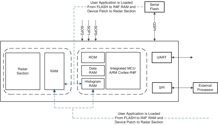
Functional Mode

In Functional Mode, the Master System’s bootloader looks for a valid image in the serial flash memory, interfaced over the QSPI port. If a valid image is found, the bootloader transfers the same to Master System’s memory subsystem. The image format contains the MSS application code and the radar subsystem patch code.

If a valid image (or the QSPI Serial Flash is not found), the bootloader initializes the SPI port and awaits for the image transfer. This operation comes handy for configurations where the IWR1443 is interfaced to an external processor which has its own nonvolatile storage hence can store the user application and the IWR1443 device’s firmware image.
IWR1443 bootloader_functional.gifFigure 6-9 Bootloader’s Functional Mode