ZHCST57 May   2023 IWR1843AOP

PRODUCTION DATA  

  1.   1
  2. 特性
  3. 应用
  4. 说明
    1. 3.1 功能方框图
  5. Revision History
  6. Device Comparison
    1. 5.1 Related Products
  7. Terminal Configuration and Functions
    1. 6.1 Pin Diagram
    2. 6.2 Pin Attributes
    3. 6.3 Signal Descriptions
      1. 6.3.1 Pin Functions - Digital and Analog [ALP Package]
  8. Specifications
    1. 7.1  Absolute Maximum Ratings
    2. 7.2  ESD Ratings
    3. 7.3  Power-On Hours (POH)
    4. 7.4  Recommended Operating Conditions
    5. 7.5  Power Supply Specifications
    6. 7.6  Power Consumption Summary
    7. 7.7  RF Specification
    8. 7.8  CPU Specifications
    9. 7.9  Thermal Resistance Characteristics for FCBGA Package [ALP0180A]
    10. 7.10 Timing and Switching Characteristics
      1. 7.10.1  Antenna Radiation Patterns
        1. 7.10.1.1 Antenna Radiation Patterns for Receiver
        2. 7.10.1.2 Antenna Radiation Patterns for Transmitter
      2. 7.10.2  Antenna Positions
      3. 7.10.3  Power Supply Sequencing and Reset Timing
      4. 7.10.4  Input Clocks and Oscillators
        1. 7.10.4.1 Clock Specifications
      5. 7.10.5  Multibuffered / Standard Serial Peripheral Interface (MibSPI)
        1. 7.10.5.1 Peripheral Description
        2. 7.10.5.2 MibSPI Transmit and Receive RAM Organization
          1. 7.10.5.2.1 SPI Timing Conditions
          2. 7.10.5.2.2 SPI Controller Mode Switching Parameters (CLOCK PHASE = 0, SPICLK = output, SPISIMO = output, and SPISOMI = input)
          3. 7.10.5.2.3 SPI Controller Mode Switching Parameters (CLOCK PHASE = 1, SPICLK = output, SPISIMO = output, and SPISOMI = input)
        3. 7.10.5.3 SPI Peripheral Mode I/O Timings
          1. 7.10.5.3.1 SPI Peripheral Mode Switching Parameters (SPICLK = input, SPISIMO = input, and SPISOMI = output)
        4. 7.10.5.4 Typical Interface Protocol Diagram (Peripheral Mode)
      6. 7.10.6  LVDS Interface Configuration
        1. 7.10.6.1 LVDS Interface Timings
      7. 7.10.7  General-Purpose Input/Output
        1. 7.10.7.1 Switching Characteristics for Output Timing versus Load Capacitance (CL) #GUID-A9917993-C388-4AAC-B9C6-6B2BF583E88E/T4362547-45 #GUID-A9917993-C388-4AAC-B9C6-6B2BF583E88E/T4362547-50
      8. 7.10.8  Controller Area Network Interface (DCAN)
        1. 7.10.8.1 Dynamic Characteristics for the DCANx TX and RX Pins
      9. 7.10.9  Controller Area Network - Flexible Data-rate (CAN-FD)
        1. 7.10.9.1 Dynamic Characteristics for the CANx TX and RX Pins
      10. 7.10.10 Serial Communication Interface (SCI)
        1. 7.10.10.1 SCI Timing Requirements
      11. 7.10.11 Inter-Integrated Circuit Interface (I2C)
        1. 7.10.11.1 I2C Timing Requirements #GUID-D26A1D00-D5E4-49AB-AFF7-B0ED1920A8A5/T4362547-185
      12. 7.10.12 Quad Serial Peripheral Interface (QSPI)
        1. 7.10.12.1 QSPI Timing Conditions
        2. 7.10.12.2 Timing Requirements for QSPI Input (Read) Timings #GUID-F4461E81-32E4-4CB7-B562-43AFC94843D1/T4362547-210 #GUID-F4461E81-32E4-4CB7-B562-43AFC94843D1/T4362547-209
        3. 7.10.12.3 QSPI Switching Characteristics
      13. 7.10.13 ETM Trace Interface
        1. 7.10.13.1 ETMTRACE Timing Conditions
        2. 7.10.13.2 ETM TRACE Switching Characteristics
      14. 7.10.14 Data Modification Module (DMM)
        1. 7.10.14.1 DMM Timing Requirements
      15. 7.10.15 JTAG Interface
        1. 7.10.15.1 JTAG Timing Conditions
        2. 7.10.15.2 Timing Requirements for IEEE 1149.1 JTAG
        3. 7.10.15.3 Switching Characteristics Over Recommended Operating Conditions for IEEE 1149.1 JTAG
  9. Detailed Description
    1. 8.1 Overview
    2. 8.2 功能方框图
    3. 8.3 Subsystems
      1. 8.3.1 RF and Analog Subsystem
        1. 8.3.1.1 Clock Subsystem
        2. 8.3.1.2 Transmit Subsystem
        3. 8.3.1.3 Receive Subsystem
      2. 8.3.2 Processor Subsystem
      3. 8.3.3 Host Interface
      4. 8.3.4 Main Subsystem Cortex-R4F Memory Map
      5. 8.3.5 DSP Subsystem Memory Map
    4. 8.4 Other Subsystems
      1. 8.4.1 ADC Channels (Service) for User Application
        1. 8.4.1.1 GP-ADC Parameter
  10. Monitoring and Diagnostics
    1. 9.1 Monitoring and Diagnostic Mechanisms
      1. 9.1.1 Error Signaling Module
  11. 10Applications, Implementation, and Layout
    1. 10.1 Application Information
    2. 10.2 Reference Schematic
  12. 11Device and Documentation Support
    1. 11.1 Device Nomenclature
    2. 11.2 Tools and Software
    3. 11.3 Documentation Support
    4. 11.4 支持资源
    5. 11.5 Trademarks
    6. 11.6 静电放电警告
    7. 11.7 术语表
  13. 12Mechanical, Packaging, and Orderable Information
    1. 12.1 Packaging Information

封装选项

机械数据 (封装 | 引脚)
散热焊盘机械数据 (封装 | 引脚)
订购信息

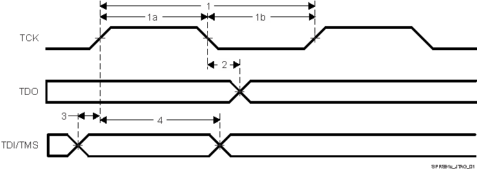
Switching Characteristics Over Recommended Operating Conditions for IEEE 1149.1 JTAG

NO.PARAMETERMINTYPMAXUNIT
2td(TCKL-TDOV)Delay time, TCK low to TDO valid025ns
GUID-9253B594-7E7B-49F2-8E63-3B9440BCA24D-low.gifFigure 7-24 JTAG Timing