ZHCSLR8B june 2021 – april 2023 JFE150
PRODUCTION DATA
- 1
- 1 特性
- 2 应用
- 3 说明
- 4 Revision History
- 5 Pin Configuration and Functions
- 6 Specifications
- 7 Parameter Measurement Information
- 8 Detailed Description
- 9 Application and Implementation
- 10Device and Documentation Support
- 11Mechanical, Packaging, and Orderable Information
9.1.4 Composite Amplifiers
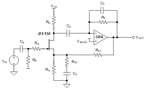
The JFE150 can be configured to provide a low-noise, high-input impedance front-end stage for a typical op amp. Open-loop transistor gain stages shown previously suffer from wide gain variations that are dependent on the forward transcondutance of the JFE150. When precision gain is required, the composite amplifier (JFET front-end + operational amplifier) achieves excellent results by allowing for a fixed gain determined by external resistors, and improving the noise and bandwidth of the operational amplifier. The JFE150 gain stage provides a boost to the open-loop performance of the system, extending the bandwidth beyond what the operational amplifier alone can provide, and gives a high-input impedance, ultra-low noise input stage to interface with high source impedance microphones.
Figure 9-6 shows a generic schematic representation of a current-feedback composite amplifier. The component requirements and tradeoffs are listed in Table 9-1.
 Figure 9-5 Low Noise, High Input
Impedance Composite Amplifier
Figure 9-5 Low Noise, High Input
Impedance Composite Amplifier| COMPONENT | DESCRIPTION | RELATED EQUATION |
|---|---|---|
| CB | DC blocking capacitor for input source. Use a dc blocking capacitor if the dc voltage of the input source is not the same as the gate bias voltage. |
Equation 2.
|
| RB | Bias resistor. Use biasing resistors to set the dc voltage at the gate. High-value resistors can be used without an impact to noise if the source impedance and bypass capacitor have sufficiently low impedance. | See Equation 2 |
| RG | Gate resistor. Can be used to help limit current flow into gate in overvoltage cases. | |
| RD | Drain resistor. Sets gain of JFET stage in common source biasing, along with gm and RS. | |
| RS | Source resistor. Used to set bias of JFET; see Figure 9-3. Resistor thermal noise directly impacts noise performance. | |
| CD | DC blocking capacitor. Blocks nominal drain voltage so the amplifier operates at a midsupply bias point. | |
| CF | Feedback capacitor. Along with RF, this capacitor sets the –3‑dB high-pass cutoff frequency when the amplifier gain-bandwidth product (GBW) is sufficiently high enough to support the –3‑dB frequency. If the GBW is not high enough, then the GBW sets the –3-dB frequency. |
Equation 3.
|
| RF | Feedback resistor. Along with CF, this resistor sets the –3‑dB high-pass cutoff frequency when the amplifier gain-bandwidth product (GBW) is sufficiently high enough to support the –3‑dB frequency. If the GBW is not high enough, then the GBW sets the –3-dB frequency. | See Equation 3 |
| RF2 | Current feedback gain-setting resistor 1. Along with RS2, sets gain closed-loop. |
Equation 4.
|
| RS2 | Current feedback gain-setting resistor 2. Along with RS2, sets gain closed-loop. Resistor thermal noise directly impacts noise performance. | See Equation 4 |
| CS | Current feedback ac-coupling capacitor. This capacitor, along with R2, sets the low-pass –3-dB frequency. |
Equation 5.
|