ZHCSKG9 November 2019 LDC1001-Q1
PRODUCTION DATA.
- 1 特性
- 2 应用
- 3 说明
- 4 修订历史记录
- 5 Pin Configuration and Functions
- 6 Specifications
-
7 Detailed Description
- 7.1 Overview
- 7.2 Functional Block Diagram
- 7.3 Feature Description
- 7.4 Device Functional Modes
- 7.5 Programming
- 7.6
Register Map
- 7.6.1
Register Description
- 7.6.1.1 Revision ID (offset = 0x00) [reset = 0x80]
- 7.6.1.2 Rp_MAX (offset = 0x01) [reset = 0x0E]
- 7.6.1.3 Rp_MIN (offset = 0x02) [reset = 0x14]
- 7.6.1.4 Sensor Frequency (offset = 0x03) [reset = 0x45]
- 7.6.1.5 LDC Configuration (offset = 0x04) [reset = 0x1B]
- 7.6.1.6 Clock Configuration (offset = 0x05) [reset = 0x01]
- 7.6.1.7 Comparator Threshold High LSB (offset = 0x06) [reset = 0xFF]
- 7.6.1.8 Comparator Threshold High MSB (offset = 0x07) [reset = 0xFF]
- 7.6.1.9 Comparator Threshold Low LSB (offset = 0x08) [reset = 0x00]
- 7.6.1.10 Comparator Threshold Low MSB (offset = 0x09) [reset = 0x00]
- 7.6.1.11 INTB Pin Configuration (offset = 0x0A) [reset = 0x00]
- 7.6.1.12 Power Configuration (offset = 0x0B) [reset = 0x00]
- 7.6.1.13 Status (offset = 0x20) [reset = NA]
- 7.6.1.14 Proximity Data LSB (offset = 0x21) [reset = NA]
- 7.6.1.15 Proximity Data MSB (offset = 0x22) [reset = NA]
- 7.6.1.16 Frequency Counter LSB (offset = 0x23) [reset = NA]
- 7.6.1.17 Frequency Counter Mid-Byte (offset = 0x24) [reset = NA]
- 7.6.1.18 Frequency Counter MSB (offset = 0x25) [reset = NA]
- 7.6.1
Register Description
- 8 Application and Implementation
- 9 Power Supply Recommendations
- 10Layout
- 11器件和文档支持
- 12机械、封装和可订购信息
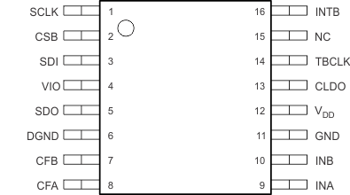
5 Pin Configuration and Functions
PW Package
16-Pin TSSOP
Top View

Pin Functions
| PIN | TYPE(1) | DESCRIPTION | |
|---|---|---|---|
| NO. | NAME | ||
| 1 | SCLK | DI | SPI clock input. The SCLK pin is used to clock-out and clock-in the data from or into the chip |
| 2 | CSB | DI | SPI CSB. Multiple devices can be connected on the same SPI bus and the CSB pin can be used to select which device is communicated with. |
| 3 | SDI | DI | SPI Slave Data In (Master Out Slave In). This pin should be connected to the Master Out Slave In of the master device. |
| 4 | VIO | P | Digital IO Supply |
| 5 | SDO | DO | SPI Slave Data Out (Master In Slave Out). This pin is high-Z when the CSB pin is high. |
| 6 | DGND | P | Digital ground |
| 7 | CFB | A | LDC filter capacitor |
| 8 | CFA | A | LDC filter capacitor |
| 9 | INA | A | External LC Tank. Connect this pin to an external LC tank. |
| 10 | INB | A | External LC Tank. Connect this pin to an external LC tank. |
| 11 | GND | P | Analog ground |
| 12 | VDD | P | Analog supply |
| 13 | CLDO | A | LDO bypass capacitor. Connect a 56-nF capacitor from this pin to GND. |
| 14 | TBCLK | DI | External time-base clock |
| 15 | NC | NC | This pin should be floating. |
| 16 | INTB | DO | Configurable interrupt. This pin can be configured to function in three different ways (threshold detect, wake-up, or DRDYB) by programing the INT pin mode register. |
(1) DO: Digital Output, DI: Digital Input, P: Power, A: Analog