ZHCSKH7 November 2019 LDC1001
PRODUCTION DATA.
- 1 特性
- 2 应用
- 3 说明
- 4 修订历史记录
- 5 Pin Configuration and Functions
- 6 Specifications
-
7 Detailed Description
- 7.1 Overview
- 7.2 Functional Block Diagram
- 7.3 Feature Description
- 7.4 Device Functional Modes
- 7.5 Programming
- 7.6
Register Maps
- 7.6.1
Register Description
- 7.6.1.1 Revision ID (Address = 0x00)
- 7.6.1.2 RP_MAX (Address = 0x01)
- 7.6.1.3 RP_MIN (Address = 0x02)
- 7.6.1.4 Watchdog Timer Frequency (Address = 0x03)
- 7.6.1.5 LDC Configuration (Address = 0x04)
- 7.6.1.6 Clock Configuration (Address = 0x05)
- 7.6.1.7 Comparator Threshold High LSB (Address = 0x06)
- 7.6.1.8 Comparator Threshold High MSB (Address = 0x07)
- 7.6.1.9 Comparator Threshold Low LSB (Address = 0x08)
- 7.6.1.10 Comparator Threshold Low MSB (Address = 0x09)
- 7.6.1.11 INTB Pin Configuration (Address = 0x0A)
- 7.6.1.12 Power Configuration (Address = 0x0B)
- 7.6.1.13 Status (Address = 0x20)
- 7.6.1.14 Proximity Data LSB (Address = 0x21)
- 7.6.1.15 Proximity Data MSB (Address = 0x22)
- 7.6.1.16 Frequency Counter LSB (Address = 0x23)
- 7.6.1.17 Frequency Counter Mid-Byte (Address = 0x24)
- 7.6.1.18 Frequency Counter MSB (Address = 0x25)
- 7.6.1
Register Description
- 8 Application and Implementation
- 9 Power Supply Recommendations
- 10Layout
- 11器件和文档支持
- 12机械、封装和可订购信息
7.5.1 SPI Description
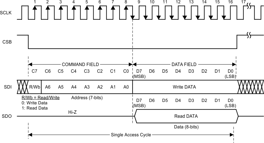
A typical serial interface transaction begins with an 8-bit instruction, which is comprised of a read/write bit (MSB, R=1) and a 7-bit address of the register, followed by a Data field which is typically 8 bits. However, the data field can be extended to a multiple of 8 bits by providing sufficient SPI clocks. Refer to the Extended SPI Transactions section for more information.
 Figure 15. Serial Interface Protocol
 Each assertion of chip select bar (CSB) starts a new register access. The R/Wb bit in the command field configures the type of the access. A value of 0 indicates a write operation, and a value of 1 indicates a read operation. All output data is driven on the falling edge of the serial clock (SCLK), and all input data is sampled on the rising edge of the serial clock (SCLK). Data is written into the register on the rising edge of the 16th clock. It is required to deassert CSB after the 16th clock. Remember that if CSB is deasserted before the 16th clock, no data write will occur.
The LDC1001 utilizes a 4-wire SPI interface to access control and data registers. The LDC1001 is an SPI slave device and does not initiate any transactions.