ZHCSHX3A December   2014  – March 2018 LDC1312 , LDC1314

PRODUCTION DATA.  

  1. 特性
  2. 应用
  3. 说明
    1.     Device Images
      1.      简化原理图
      2.      测量精度与目标距离间的关系
  4. 修订历史记录
  5. Pin Configuration and Functions
    1.     Pin Functions
  6. Specifications
    1. 6.1 Absolute Maximum Ratings
    2. 6.2 ESD Ratings
    3. 6.3 Recommended Operating Conditions
    4. 6.4 Thermal Information
    5. 6.5 Electrical Characteristics
    6. 6.6 Switching Characteristics - I2C
    7. 6.7 Typical Characteristics
  7. Detailed Description
    1. 7.1 Overview
    2. 7.2 Functional Block Diagram
    3. 7.3 Feature Description
      1. 7.3.1 Multi-Channel and Single Channel Operation
      2. 7.3.2 Adjustable Conversion Time
      3. 7.3.3 Digital Signal Gain
      4. 7.3.4 Sensor Startup and Glitch Configuration
      5. 7.3.5 Reference Clock
      6. 7.3.6 Sensor Current Drive Control
      7. 7.3.7 Device Status Monitoring
    4. 7.4 Device Functional Modes
      1. 7.4.1 Startup Mode
      2. 7.4.2 Sleep Mode (Configuration Mode)
      3. 7.4.3 Normal (Conversion) Mode
      4. 7.4.4 Shutdown Mode
        1. 7.4.4.1 Reset
    5. 7.5 Programming
      1. 7.5.1 I2C Interface Specifications
      2. 7.5.2 Pulses on I2C
    6. 7.6 Register Maps
      1. 7.6.1  Register List
      2. 7.6.2  Address 0x00, DATA0
        1. Table 1. Address 0x00, DATA0 Field Descriptions
      3. 7.6.3  Address 0x02, DATA1
        1. Table 2. Address 0x02, DATA1 Field Descriptions
      4. 7.6.4  Address 0x04, DATA2 (LDC1314 only)
        1. Table 3. Address 0x04, DATA2 Field Descriptions
      5. 7.6.5  Address 0x06, DATA3 (LDC1314 only)
        1. Table 4. Address 0x06, DATA3 Field Descriptions
      6. 7.6.6  Address 0x08, RCOUNT0
        1. Table 5. Address 0x08, RCOUNT0 Field Descriptions
      7. 7.6.7  Address 0x09, RCOUNT1
        1. Table 6. Address 0x09, RCOUNT1 Field Descriptions
      8. 7.6.8  Address 0x0A, RCOUNT2 (LDC1314 only)
        1. Table 7. Address 0x0A, RCOUNT2 Field Descriptions
      9. 7.6.9  Address 0x0B, RCOUNT3 (LDC1314 only)
        1. Table 8. Address 0x0B, RCOUNT3 Field Descriptions
      10. 7.6.10 Address 0x0C, OFFSET0
        1. Table 9. OFFSET0 Field Descriptions
      11. 7.6.11 Address 0x0D, OFFSET1
        1. Table 10. Address 0x0D, OFFSET1 Field Descriptions
      12. 7.6.12 Address 0x0E, OFFSET2 (LDC1314 only)
        1. Table 11. Address 0x0E, OFFSET2 Field Descriptions
      13. 7.6.13 Address 0x0F, OFFSET3 (LDC1314 only)
        1. Table 12. Address 0x0F, OFFSET3 Field Descriptions
      14. 7.6.14 Address 0x10, SETTLECOUNT0
        1. Table 13. Address 0x10, SETTLECOUNT0 Field Descriptions
      15. 7.6.15 Address 0x11, SETTLECOUNT1
        1. Table 14. Address 0x11, SETTLECOUNT1 Field Descriptions
      16. 7.6.16 Address 0x12, SETTLECOUNT2 (LDC1314 only)
        1. Table 15. Address 0x12, SETTLECOUNT2 Field Descriptions
      17. 7.6.17 Address 0x13, SETTLECOUNT3 (LDC1314 only)
        1. Table 16. Address 0x13, SETTLECOUNT3 Field Descriptions
      18. 7.6.18 Address 0x14, CLOCK_DIVIDERS0
        1. Table 17. Address 0x14, CLOCK_DIVIDERS0 Field Descriptions
      19. 7.6.19 Address 0x15, CLOCK_DIVIDERS1
        1. Table 18. Address 0x15, CLOCK_DIVIDERS1 Field Descriptions
      20. 7.6.20 Address 0x16, CLOCK_DIVIDERS2 (LDC1314 only)
        1. Table 19. Address 0x16, CLOCK_DIVIDERS2 Field Descriptions
      21. 7.6.21 Address 0x17, CLOCK_DIVIDERS3 (LDC1314 only)
        1. Table 20. Address 0x17, CLOCK_DIVIDERS3
      22. 7.6.22 Address 0x18, STATUS
        1. Table 21. Address 0x18, STATUS Field Descriptions
      23. 7.6.23 Address 0x19, ERROR_CONFIG
        1. Table 22. Address 0x19, ERROR_CONFIG
      24. 7.6.24 Address 0x1A, CONFIG
        1. Table 23. Address 0x1A, CONFIG Field Descriptions
      25. 7.6.25 Address 0x1B, MUX_CONFIG
        1. Table 24. Address 0x1B, MUX_CONFIG Field Descriptions
      26. 7.6.26 Address 0x1C, RESET_DEV
        1. Table 25. Address 0x1C, RESET_DEV Field Descriptions
      27. 7.6.27 Address 0x1E, DRIVE_CURRENT0
        1. Table 26. Address 0x1E, DRIVE_CURRENT0 Field Descriptions
      28. 7.6.28 Address 0x1F, DRIVE_CURRENT1
        1. Table 27. Address 0x1F, DRIVE_CURRENT1 Field Descriptions
      29. 7.6.29 Address 0x20, DRIVE_CURRENT2 (LDC1314 only)
        1. Table 28. Address 0x20, DRIVE_CURRENT2 Field Descriptions
      30. 7.6.30 Address 0x21, DRIVE_CURRENT3 (LDC1314 only)
        1. Table 29. DRIVE_CURRENT3 Field Descriptions
      31. 7.6.31 Address 0x7E, MANUFACTURER_ID
        1. Table 30. Address 0x7E, MANUFACTURER_ID Field Descriptions
      32. 7.6.32 Address 0x7F, DEVICE_ID
        1. Table 31. Address 0x7F, DEVICE_ID Field Descriptions
  8. Application and Implementation
    1. 8.1 Application Information
      1. 8.1.1 Conductive Objects in a Time-Varying EM Field
      2. 8.1.2 L-C Resonators
      3. 8.1.3 Multi-Channel and Single Channel Operation
        1. 8.1.3.1 Data Offset
        2. 8.1.3.2 Digital Signal Gain
      4. 8.1.4 Sensor Conversion Time
        1. 8.1.4.1 Settling Time
        2. 8.1.4.2 Sensor Activation
      5. 8.1.5 Sensor Current Drive Configuration
        1. 8.1.5.1 Inactive Channel Sensor Connections
        2. 8.1.5.2 Automatic IDRIVE Setting with RP_OVERRIDE_EN
        3. 8.1.5.3 Determining Sensor IDRIVE for an Unknown Sensor RP Using an Oscilloscope
        4. 8.1.5.4 Sensor Auto-Calibration Mode
        5. 8.1.5.5 Channel 0 High Current Drive
      6. 8.1.6 Clocking Architecture
      7. 8.1.7 Input Deglitch Filter
      8. 8.1.8 Device Status Registers
      9. 8.1.9 Multi-Channel Data Readback
    2. 8.2 Typical Application
      1. 8.2.1 System Sensing Functionality
      2. 8.2.2 Example Application
      3. 8.2.3 Design Requirements
      4. 8.2.4 Detailed Design Procedure
      5. 8.2.5 Recommended Initial Register Configuration Values
      6. 8.2.6 Application Curves
      7. 8.2.7 Inductor Self-Resonant Frequency
  9. Power Supply Recommendations
  10. 10Layout
    1. 10.1 Layout Guidelines
    2. 10.2 Layout Example
  11. 11器件和文档支持
    1. 11.1 器件支持
      1. 11.1.1 开发支持
    2. 11.2 文档支持
      1. 11.2.1 相关文档
    3. 11.3 相关链接
    4. 11.4 接收文档更新通知
    5. 11.5 社区资源
    6. 11.6 商标
    7. 11.7 静电放电警告
    8. 11.8 Glossary
  12. 12机械、封装和可订购信息

封装选项

机械数据 (封装 | 引脚)
散热焊盘机械数据 (封装 | 引脚)
订购信息

Digital Signal Gain

Internally, the LDC measures inductance shifts with 16 bits of resolution, while the conversion output word width is only 12 bits. For systems in which the sensor signal variation is less than 25% of the full scale range, the LDC can report conversion results with higher resolution by setting the Output Gain. The Output Gain is applied to all device channels. An output gain can be used to apply a 2-bit, 3-bit, or 4-bit shift to the output code for all channels, providing an effectively higher measurement resolution. When the Gain function is used, additional LSBs of the conversion word are reported, while the corresponding number of MSBs are not reported.

To avoid data corruption issues, use the Output Gain function (Data Offset) to shift the output codes to prevent toggling of the shifted MSBs.

Table 35. Output Gain Register

CHANNEL(1) REGISTER FIELD [ BIT(S) ] VALUES EFFECTIVE RESOLUTION (BITS) OUTPUT RANGE
All RESET_DEV, addr 0x1C OUTPUT_GAIN [ 10:9 ] 00 (default): Gain =1 (0 bits shift) 12 100% full scale
01: Gain = 4 (2 bits left shift) 14 25% full scale
10: Gain = 8 (3 bits left shift) 15 12.5% full scale
11 : Gain = 16 (4 bits left shift) 16 6.25% full scale
Channels 2 and 3 are available for LDC1314 only.

Example: If the conversion result for a channel is 0x07A3, with OUTPUT_GAIN=0x0, the reported output code is 0x07A. If OUTPUT_GAIN is set to 0x3 in the same condition, then the reported output code is 0x7A3. The original 4 MSBs (0x0) are no longer accessible. Figure 51 illustrates the segments of the 16-bit sample that is reported for each possible gain setting.
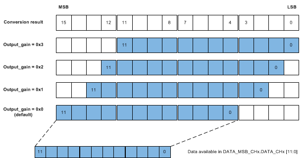
LDC1312 LDC1314 conversion_data_output_gain_snoscy9.gifFigure 51. Conversion Data Output Gain