ZHCSHX3A December 2014 – March 2018 LDC1312 , LDC1314
PRODUCTION DATA.
- 1 特性
- 2 应用
- 3 说明
- 4 修订历史记录
- 5 Pin Configuration and Functions
- 6 Specifications
-
7 Detailed Description
- 7.1 Overview
- 7.2 Functional Block Diagram
- 7.3 Feature Description
- 7.4 Device Functional Modes
- 7.5 Programming
- 7.6
Register Maps
- 7.6.1 Register List
- 7.6.2 Address 0x00, DATA0
- 7.6.3 Address 0x02, DATA1
- 7.6.4 Address 0x04, DATA2 (LDC1314 only)
- 7.6.5 Address 0x06, DATA3 (LDC1314 only)
- 7.6.6 Address 0x08, RCOUNT0
- 7.6.7 Address 0x09, RCOUNT1
- 7.6.8 Address 0x0A, RCOUNT2 (LDC1314 only)
- 7.6.9 Address 0x0B, RCOUNT3 (LDC1314 only)
- 7.6.10 Address 0x0C, OFFSET0
- 7.6.11 Address 0x0D, OFFSET1
- 7.6.12 Address 0x0E, OFFSET2 (LDC1314 only)
- 7.6.13 Address 0x0F, OFFSET3 (LDC1314 only)
- 7.6.14 Address 0x10, SETTLECOUNT0
- 7.6.15 Address 0x11, SETTLECOUNT1
- 7.6.16 Address 0x12, SETTLECOUNT2 (LDC1314 only)
- 7.6.17 Address 0x13, SETTLECOUNT3 (LDC1314 only)
- 7.6.18 Address 0x14, CLOCK_DIVIDERS0
- 7.6.19 Address 0x15, CLOCK_DIVIDERS1
- 7.6.20 Address 0x16, CLOCK_DIVIDERS2 (LDC1314 only)
- 7.6.21 Address 0x17, CLOCK_DIVIDERS3 (LDC1314 only)
- 7.6.22 Address 0x18, STATUS
- 7.6.23 Address 0x19, ERROR_CONFIG
- 7.6.24 Address 0x1A, CONFIG
- 7.6.25 Address 0x1B, MUX_CONFIG
- 7.6.26 Address 0x1C, RESET_DEV
- 7.6.27 Address 0x1E, DRIVE_CURRENT0
- 7.6.28 Address 0x1F, DRIVE_CURRENT1
- 7.6.29 Address 0x20, DRIVE_CURRENT2 (LDC1314 only)
- 7.6.30 Address 0x21, DRIVE_CURRENT3 (LDC1314 only)
- 7.6.31 Address 0x7E, MANUFACTURER_ID
- 7.6.32 Address 0x7F, DEVICE_ID
-
8 Application and Implementation
- 8.1
Application Information
- 8.1.1 Conductive Objects in a Time-Varying EM Field
- 8.1.2 L-C Resonators
- 8.1.3 Multi-Channel and Single Channel Operation
- 8.1.4 Sensor Conversion Time
- 8.1.5 Sensor Current Drive Configuration
- 8.1.6 Clocking Architecture
- 8.1.7 Input Deglitch Filter
- 8.1.8 Device Status Registers
- 8.1.9 Multi-Channel Data Readback
- 8.2 Typical Application
- 8.1
Application Information
- 9 Power Supply Recommendations
- 10Layout
- 11器件和文档支持
- 12机械、封装和可订购信息
8.1.6 Clocking Architecture
Optimum LDC1312/LDC1314 performance requires a clean reference clock with a limited frequency range. The device provides digital dividers for the ƒCLK and the sensor inputs. The dividers provide flexibility in system design, so that the full range of sensor frequencies can be supported with available fCLK. Each channel has a dedicated divider configuration. Higher reference frequencies provide a higher sample rate for a given resolution.
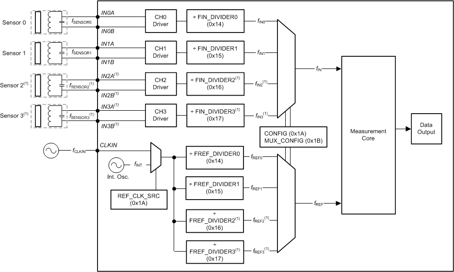
Figure 54 shows the clock dividers and multiplexers of the LDC.
 Figure 54. Clocking Diagram
(1) LDC1314 only
In Figure 54, the key clocks are ƒINx, ƒREFx, and ƒCLK. ƒCLK is selected from either the internal clock source or external clock source (CLKIN). The frequency measurement reference clock, ƒREF, is derived from the ƒCLK source.
The internal oscillator is highly stable across temperature and is suitable for most LDC1312/4 applications. Applications requiring matched performance across multiple LDC1312/4 devices and/or requiring higher long-term stability may need an external oscillator. Note that some internal functions, such as watchdog timers, always use ƒINT for timing.
The ƒINx clock is derived from sensor frequency for channel x, ƒSENSORx. ƒREFx and ƒINx must meet the requirements listed in Table 40, depending on whether ƒCLK (reference clock) is the internal or external clock.
Table 40. Clock Frequency Requirements
| MODE(1) | REFERENCE SOURCE | VALID ƒREFx RANGE | VALID ƒINx RANGE | SET FIN_DIVIDERx to | VALID SETTLECOUNTx SETTINGS | VALID RCOUNTx SETTINGS |
|---|---|---|---|---|---|---|
| Multi-Channel | Internal | ƒREFx≤ 55 MHz | < ƒREFx /4 | ≥ b0001 (2) | > 3 | > 8 |
| External | ƒREFx ≤ 40 MHz | |||||
| Single-Channel | Either external or internal | ƒREFx ≤ 35 MHz |
Table 41 shows the clock configuration registers. Each input channel has a dedicated configuration which can be set independently.
Table 41. Clock Configuration Registers
| CHANNEL(1) | CLOCK | REGISTER | FIELD | VALUE |
|---|---|---|---|---|
| All | ƒCLK = Reference Clock Source | CONFIG, addr 0x1A | REF_CLK_SRC [9] | b0 = internal oscillator is used as the reference clock
b1 = external clock source is used as the reference clock |
| 0 | ƒREF0 | CLOCK_DIVIDERS0, addr 0x14 | FREF_DIVIDER0 [9:0] | ƒREF0 = ƒCLK / FREF_DIVIDER0 |
| 1 | ƒREF1 | CLOCK_DIVIDERS1, addr 0x15 | FREF_DIVIDER1 [9:0] | ƒREF1 = ƒCLK / FREF_DIVIDER1 |
| 2 | ƒREF2 | CLOCK_DIVIDERS2, addr 0x16 | FREF_DIVIDER2 [9:0] | ƒREF2 = ƒCLK / FREF_DIVIDER2 |
| 3 | ƒREF3 | CLOCK_DIVIDERS3, addr 0x17 | FREF_DIVIDER3 [9:0] | ƒREF3 = ƒCLK / FREF_DIVIDER3 |
| 0 | ƒIN0 | CLOCK_DIVIDERS0, addr 0x14 | FIN_DIVIDER0 [15:12] | ƒIN0 = ƒSENSOR0 / FIN_DIVIDER0 |
| 1 | ƒIN1 | CLOCK_DIVIDERS1, addr 0x15 | FIN_DIVIDER1 [15:12] | ƒIN1 = ƒSENSOR1 / FIN_DIVIDER1 |
| 2 | ƒIN2 | CLOCK_DIVIDERS2, addr 0x16 | FIN_DIVIDER2 [15:12] | ƒIN2 = ƒSENSOR2 / FIN_DIVIDER2 |
| 3 | ƒIN3 | CLOCK_DIVIDERS3, addr 0x17 | FIN_DIVIDER3 [15:12] | ƒIN3 = ƒSENSOR3 / FIN_DIVIDER3 |