ZHCSM23 December 2021 LDC3114
PRODUCTION DATA
- 1 特性
- 2 应用
- 3 说明
- 4 Revision History
- 5 Pin Configuration and Functions
- 6 Specifications
-
7 Detailed Description
- 7.1 Overview
- 7.2 Functional Block Diagram
- 7.3 Feature Description
- 7.4 Device Functional Modes
- 7.5 Register Maps
-
8 Application and Implementation
- 8.1
Application Information
- 8.1.1 Theory of Operation
- 8.1.2 Designing Sensor Parameters
- 8.1.3 Setting COM Pin Capacitor
- 8.1.4 Defining Power-On Timing
- 8.1.5 Configuring Button or Raw Data Scan Rate
- 8.1.6 Programming Button or Raw Data Sampling Window
- 8.1.7 Scaling Frequency Counter Output
- 8.1.8 Setting Button Triggering Threshold
- 8.1.9 Tracking Baseline
- 8.1.10 Mitigating False Button Detections
- 8.1.11 Reporting Interrupts for Button Presses, Raw Data Ready and Error Conditions
- 8.1.12 Estimating Supply Current
- 8.2 Typical Application
- 8.1
Application Information
- 9 Power Supply Recommendations
- 10Layout
- 11Device and Documentation Support
- 12Mechanical, Packaging, and Orderable Information
7.3.8.1 I2C Interface Specifications
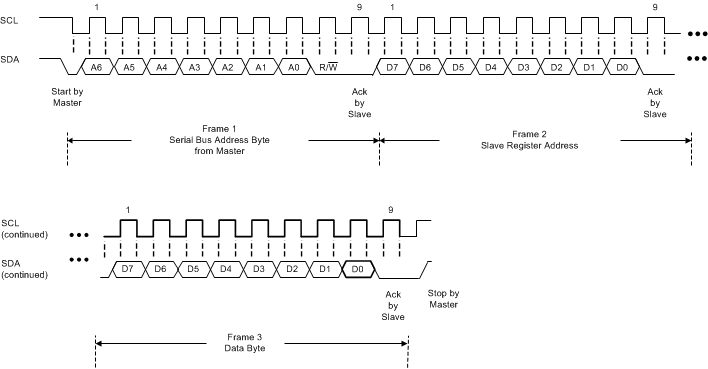
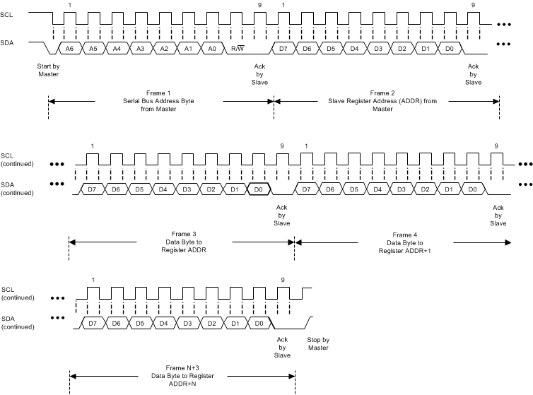
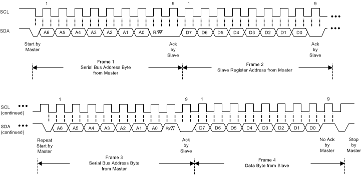
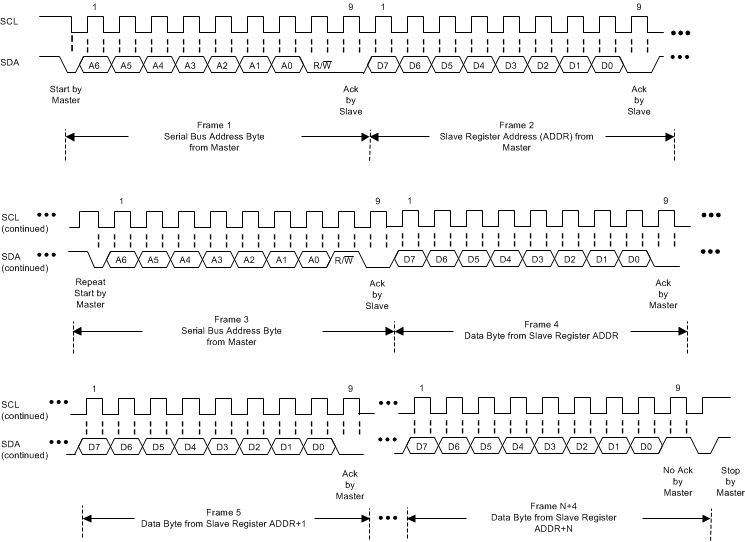
The maximum speed of the I2C interface is 400 kHz. This sequence uses the standard I2C 7-bit target address followed by an 8-bit pointer to set the register address. For both write and read, the address pointer will auto-increment as long as the controller acknowledges.
 Figure 7-4 I2C Sequence of Writing a Single Register
 Figure 7-5 I2C Sequence of Writing Consecutive Registers
 Figure 7-6 I2C Sequence of Reading a Single Register
 Figure 7-7 I2C Sequence of Reading Consecutive Registers