ZHCSJ59C december   2018  – july 2023 LDC5072-Q1

PRODUCTION DATA  

  1.   1
  2. 特性
  3. 应用
  4. 说明
  5. Revision History
  6. 说明(续)
  7. Pin Configuration and Functions
  8. Specifications
    1. 7.1 Absolute Maximum Ratings
    2. 7.2 ESD Ratings
    3. 7.3 Recommended Operating Conditions
    4. 7.4 Thermal Information
    5. 7.5 Electrical Characteristics
    6. 7.6 Diagnostics
    7. 7.7 Switching Characteristics
    8. 7.8 Typical Characteristics
  9. Detailed Description
    1. 8.1 Overview
    2. 8.2 Functional Block Diagram
    3. 8.3 Feature Description
      1. 8.3.1 Input Supply Voltage
      2. 8.3.2 Excitation Signal
      3. 8.3.3 Signal Processing Block
        1. 8.3.3.1 Demodulation
        2. 8.3.3.2 Fixed Gain Control
        3. 8.3.3.3 Automatic Gain Control
      4. 8.3.4 Output Stage
      5. 8.3.5 Diagnostics
        1. 8.3.5.1 Undervoltage Diagnostics
        2. 8.3.5.2 Initialization Diagnostics
        3. 8.3.5.3 Normal State Diagnostics
        4. 8.3.5.4 Fault State Diagnostics
    4. 8.4 Device Functional Modes
      1. 8.4.1 IDLE State
      2. 8.4.2 DIAGNOSTICS State
      3. 8.4.3 NORMAL State
      4. 8.4.4 FAULT State
      5. 8.4.5 DISABLED State
  10. Application and Implementation
    1. 9.1 Application Information
    2. 9.2 Typical Applications
      1. 9.2.1 5-V Supply Mode
        1. 9.2.1.1 Design Requirements
        2. 9.2.1.2 Detailed Design Procedure
          1. 9.2.1.2.1 VREG and VCC
          2. 9.2.1.2.2 Output Capacitors
          3. 9.2.1.2.3 AGC Mode
        3. 9.2.1.3 Application Curve
      2. 9.2.2 3.3-V Supply Mode
        1. 9.2.2.1 Design Requirements
        2. 9.2.2.2 Detailed Design Procedure
          1. 9.2.2.2.1 VREG and VCC
          2. 9.2.2.2.2 Output Capacitors
          3. 9.2.2.2.3 Fixed Gain Mode
      3. 9.2.3 Redundancy Mode
      4. 9.2.4 Single-Ended Mode
      5. 9.2.5 External Diagnostics Required for Loss of VCC or GND
  11. 10Power Supply Recommendations
    1. 10.1 Mode 1: VCC = 5 V, VREG = 3.3 V
    2. 10.2 Mode 2: VCC = VREG = 3.3 V
  12. 11Layout
    1. 11.1 Layout Guidelines
    2. 11.2 Layout Example
  13. 12Device and Documentation Support
    1. 12.1 Receiving Notification of Documentation Updates
    2. 12.2 支持资源
    3. 12.3 Trademarks
    4. 12.4 静电放电警告
    5. 12.5 术语表
  14. 13Mechanical, Packaging, and Orderable Information

封装选项

机械数据 (封装 | 引脚)
散热焊盘机械数据 (封装 | 引脚)
订购信息

Excitation Signal

The excitation signal is generated by an LC oscillator. The LCIN and LCOUT pins will be connected to the excitation coil. The oscillator signal driver automatically regulates the signal to VAMP_LC. The user can adjust the external capacitors on LCIN and LCOUT to select the excitation frequency. For best performance, two capacitors should be used. One should be placed from LCIN to ground and the other from LCOUT to ground (C1 and C2). This is instead of using one capacitor between LCIN and LCOUT.

Use Equation 1 to calculate the excitation frequency.

Equation 1. GUID-C1D8E1E5-EA18-4F7E-9533-400E2900B9E2-low.gif
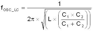
where

  • L is inductance of excitation coil
  • C1, C2 are the external capacitors on LCIN and LCOUT, respectively