ZHCSJ59C december   2018  – july 2023 LDC5072-Q1

PRODUCTION DATA  

  1.   1
  2. 特性
  3. 应用
  4. 说明
  5. Revision History
  6. 说明(续)
  7. Pin Configuration and Functions
  8. Specifications
    1. 7.1 Absolute Maximum Ratings
    2. 7.2 ESD Ratings
    3. 7.3 Recommended Operating Conditions
    4. 7.4 Thermal Information
    5. 7.5 Electrical Characteristics
    6. 7.6 Diagnostics
    7. 7.7 Switching Characteristics
    8. 7.8 Typical Characteristics
  9. Detailed Description
    1. 8.1 Overview
    2. 8.2 Functional Block Diagram
    3. 8.3 Feature Description
      1. 8.3.1 Input Supply Voltage
      2. 8.3.2 Excitation Signal
      3. 8.3.3 Signal Processing Block
        1. 8.3.3.1 Demodulation
        2. 8.3.3.2 Fixed Gain Control
        3. 8.3.3.3 Automatic Gain Control
      4. 8.3.4 Output Stage
      5. 8.3.5 Diagnostics
        1. 8.3.5.1 Undervoltage Diagnostics
        2. 8.3.5.2 Initialization Diagnostics
        3. 8.3.5.3 Normal State Diagnostics
        4. 8.3.5.4 Fault State Diagnostics
    4. 8.4 Device Functional Modes
      1. 8.4.1 IDLE State
      2. 8.4.2 DIAGNOSTICS State
      3. 8.4.3 NORMAL State
      4. 8.4.4 FAULT State
      5. 8.4.5 DISABLED State
  10. Application and Implementation
    1. 9.1 Application Information
    2. 9.2 Typical Applications
      1. 9.2.1 5-V Supply Mode
        1. 9.2.1.1 Design Requirements
        2. 9.2.1.2 Detailed Design Procedure
          1. 9.2.1.2.1 VREG and VCC
          2. 9.2.1.2.2 Output Capacitors
          3. 9.2.1.2.3 AGC Mode
        3. 9.2.1.3 Application Curve
      2. 9.2.2 3.3-V Supply Mode
        1. 9.2.2.1 Design Requirements
        2. 9.2.2.2 Detailed Design Procedure
          1. 9.2.2.2.1 VREG and VCC
          2. 9.2.2.2.2 Output Capacitors
          3. 9.2.2.2.3 Fixed Gain Mode
      3. 9.2.3 Redundancy Mode
      4. 9.2.4 Single-Ended Mode
      5. 9.2.5 External Diagnostics Required for Loss of VCC or GND
  11. 10Power Supply Recommendations
    1. 10.1 Mode 1: VCC = 5 V, VREG = 3.3 V
    2. 10.2 Mode 2: VCC = VREG = 3.3 V
  12. 11Layout
    1. 11.1 Layout Guidelines
    2. 11.2 Layout Example
  13. 12Device and Documentation Support
    1. 12.1 Receiving Notification of Documentation Updates
    2. 12.2 支持资源
    3. 12.3 Trademarks
    4. 12.4 静电放电警告
    5. 12.5 术语表
  14. 13Mechanical, Packaging, and Orderable Information

封装选项

机械数据 (封装 | 引脚)
散热焊盘机械数据 (封装 | 引脚)
订购信息

Signal Processing Block

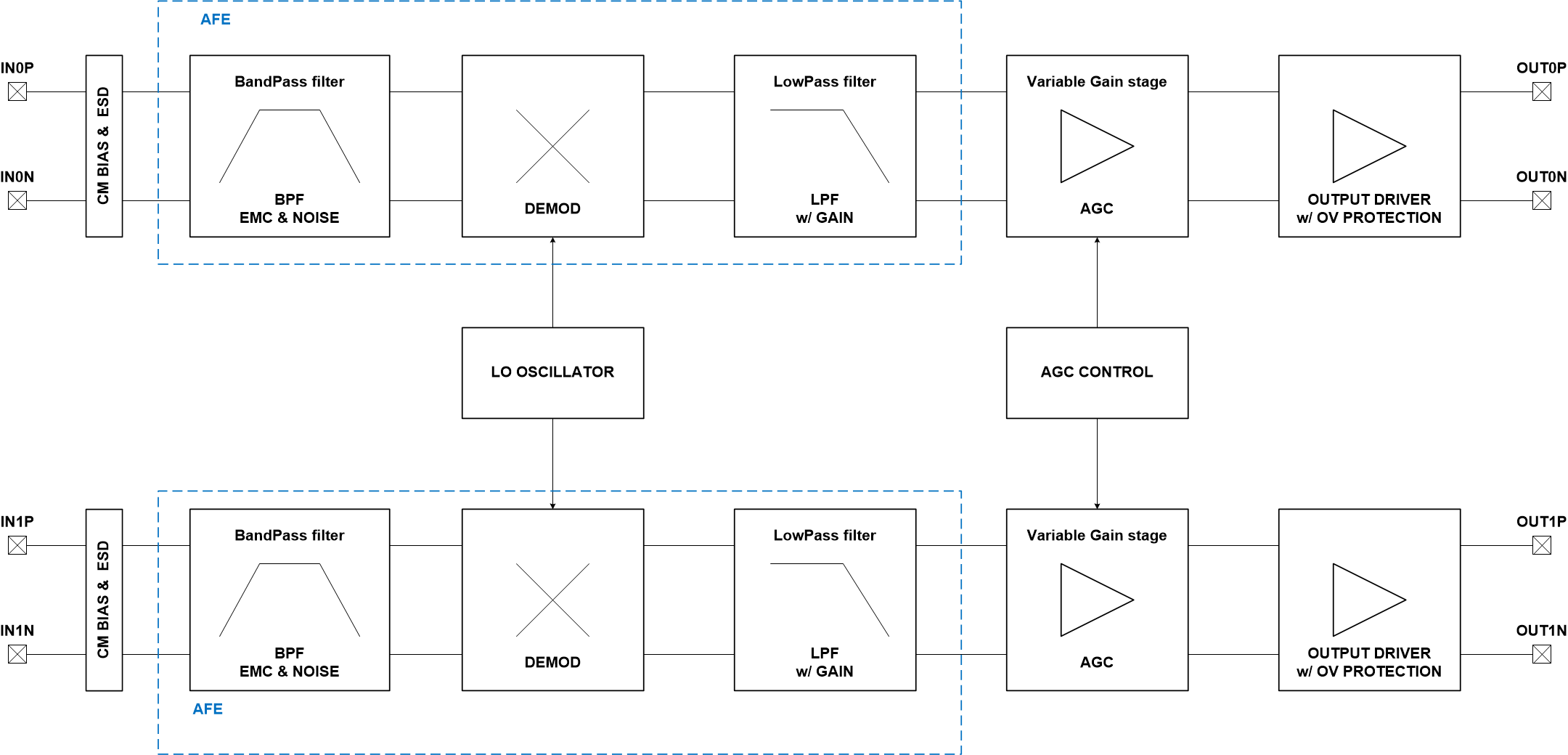
The inputs to the signal processing block come from the outputs of the receiver coils of the position sensor. This block will demodulate the position signals, filter out noise, and amplify the signal in preparation for angle calculation by an external control unit. The first stage of the signal processing block contains ESD protection circuitry and sets the common-mode voltage. The second stage of this block is an EMC filter to eliminate noise. The next stage of this block is a demodulator for the input signals. This demodulation uses the frequency of the LC oscillator as a reference. The signals will then go through a low-pass filter with fixed gain. The last stage in the signal processing block is a gain stage where the gain is either set by an automatic gain control routine (AGC_EN pin pulled to GND through an external resistor), or set to a fixed gain by the voltage on the AGC_EN pin. The signal path gain for both channels is same and are matched very closely by careful design.

Figure 8-2 shows a block diagram of the analog front-end in the IC that demodulates the incoming signal to extract position information.
GUID-BF189F71-E5F5-413F-BCC3-E9B80FE3655F-low.gif Figure 8-2 Signal Processing Block Diagram