ZHCSJ59C december 2018 – july 2023 LDC5072-Q1
PRODUCTION DATA
- 1
- 1 特性
- 2 应用
- 3 说明
- 4 Revision History
- 5 说明(续)
- 6 Pin Configuration and Functions
- 7 Specifications
- 8 Detailed Description
- 9 Application and Implementation
- 10Power Supply Recommendations
- 11Layout
- 12Device and Documentation Support
- 13Mechanical, Packaging, and Orderable Information
8.4 Device Functional Modes
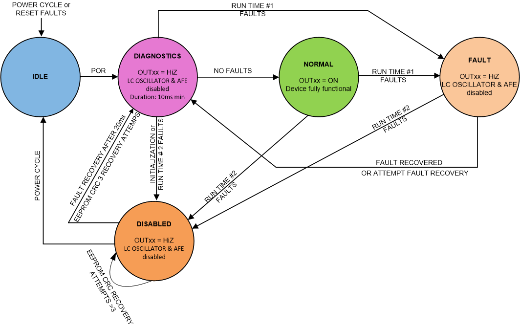
The LDC5072-Q1 is driven by a state machine. The state machine is initialized upon power up, and the machine goes through the initial diagnostics routines. If the system functions normally, the device moves to a normal operational state and starts to drive the OUT pin to indicate angular information. In case of a fault, the device moves to the FAULT state, the LC oscillator driver is disabled, and the OUT pins are tri-stated to indicate fault condition until the FAULT condition is removed or the IC is power-cycled. Some critical faults will lead to the disabled state, which requires a power-cycle to recover.
Figure 8-5 shows the different device states. The management of faults is divided into four types of faults as shown in Table 8-1:
- Initialization faults: These faults occur during initialization and transitions the device to DISABLED state and the device indicates a fault at the OUTx pins.
- Run Time #1 faults: These faults are checked in NORMAL state and transition the device to FAULT state. For these type of faults, the device will try to recover from FAULT state when the fault condition is removed and by transitioning to the DIAGNOSTIC state.
- Run Time #2 faults: These faults are critical faults which are checked in NORMAL state and transition to DISABLED state. A recovery is attempted from this state as described in DISABLED StateDISABLED StateDISABLED State.
- Reset faults: These faults will put the part in reset and the device will power up again once the conditions causing the fault are cleared.
| RESET FAULTS | INITIALIZATION FAULTS | RUN TIME FAULTS # 1 | RUN TIME FAULTS # 2 |
|---|---|---|---|
| VREG UNDER VOLTAGE CHECK | EE CRC CHECK | VCC OV/UV CHECK(1) | CRITICAL REGISTERS REDUNDANCY CHECK |
| DVDD UNDER VOLTAGE CHECK | LBIST CHECK | FREQUENCY CHECK | REGISTER CRC CHECK |
| ABIST CHECK | LC OSCILLATOR VOLTAGE CHECK | TM0 PULL UP CHECK | |
| SENSOR INTERFAFE BIST CHECK | PHASE IMBALANCE CHECK | T0UT PULL UP CHECK | |
| VREG CAP LOSS CHECK | INPUT SIGNAL OUT OF RANGE CHECK | AGC_EN TOGGLE CHECK | |
| AGC_EN BIST CHECK | OUTPUT SIGNAL OUT OF RANGE CHECK | ||
| OUTPUT SIGNAL VOLTAGE CHECK | |||
| OUTPUT SIGNAL COMMON MODE CHECK | |||
| OUTPUT SHORT CHECK | |||
| FREQUENCY IMBALANCE CHECK | |||
| TSD CHECK(1) | |||
| VREG OV CHECK(1) |
Figure 8-5 shows the states and the transitions for the LDC5072-Q1. Following states are considered SAFE state where the device has detected a fault and indicates a fault making all the OUT pins high-impedance:
- IDLE
- FAULT
- DISABLED
 Figure 8-5 Device State Diagram