SLOS013C March 1987 – March 2016 LF347 , LF347B
PRODUCTION DATA.
- 1 Features
- 2 Applications
- 3 Description
- 4 Revision History
- 5 Pin Configuration and Functions
- 6 Specifications
- 7 Parameter Measurement Information
- 8 Detailed Description
- 9 Application and Implementation
- 10Power Supply Recommendations
- 11Layout
- 12Device and Documentation Support
- 13Mechanical, Packaging, and Orderable Information
封装选项
请参考 PDF 数据表获取器件具体的封装图。
机械数据 (封装 | 引脚)
- D|14
- N|14
散热焊盘机械数据 (封装 | 引脚)
订购信息
6 Specifications
6.1 Absolute Maximum Ratings
over operating free-air temperature range (unless otherwise noted)(1)| MIN | MAX | UNIT | ||
|---|---|---|---|---|
| VCC+ | Supply voltage | 18 | V | |
| VCC– | Supply voltage | –18 | V | |
| VID | Differential input voltage | –30 | 30 | V |
| VI | Input voltage(2) | –15 | 15 | V |
| Lead temperature 1,6 mm (1/16 inch) from case for 10 seconds | 260 | °C | ||
| TJ | Operating virtual junction temperature | 150 | °C | |
| Tstg | Storage temperature | –65 | 150 | °C |
(1) Stresses beyond those listed under Absolute Maximum Ratings may cause permanent damage to the device. These are stress ratings only, which do not imply functional operation of the device at these or any other conditions beyond those indicated under Recommended Operating Conditions. Exposure to absolute-maximum-rated conditions for extended periods may affect device reliability.
(2) Unless otherwise specified, the absolute maximum negative input voltage is equal to the negative power supply voltage.
6.2 ESD Ratings
| VALUE | UNIT | |||
|---|---|---|---|---|
| V(ESD) | Electrostatic discharge | Human-body model (HBM), per ANSI/ESDA/JEDEC JS-001(1) | ±2000 | V |
| Charged-device model (CDM), per JEDEC specification JESD22-C101(2) | ±1000 | |||
(1) JEDEC document JEP155 states that 500-V HBM allows safe manufacturing with a standard ESD control process.
(2) JEDEC document JEP157 states that 250-V CDM allows safe manufacturing with a standard ESD control process.
6.3 Recommended Operating Conditions
over operating free-air temperature range (unless otherwise noted)| MIN | MAX | UNIT | ||
|---|---|---|---|---|
| TA | free-air temperature | 0 | 70 | °C |
| VCC+ | Supply voltage | 3.5 | 18 | V |
| VCC– | Supply voltage | –3.5 | –18 | V |
| VCM | Common-mode voltage | VCC– + 4 | VCC+ – 4 | V |
| TA | Operating temperature | 0 | 70 | °C |
6.4 Thermal Information
| THERMAL METRIC(1) | LF347, LF347B | UNIT | ||
|---|---|---|---|---|
| D (SOIC) | N (PDIP) | |||
| 14 PINS | 14 PINS | |||
| RθJA | Junction-to-ambient thermal resistance | 74.4 | 42.7 | °C/W |
| RθJC(top) | Junction-to-case (top) thermal resistance | 32.5 | 29.2 | °C/W |
| RθJB | Junction-to-board thermal resistance | 28.9 | 22.6 | °C/W |
| ψJT | Junction-to-top characterization parameter | 3.7 | 13.5 | °C/W |
| ψJB | Junction-to-board characterization parameter | 28.6 | 22.5 | °C/W |
(1) For more information about traditional and new thermal metrics, see the Semiconductor and IC Package Thermal Metrics application report, SPRA953.
6.5 Electrical Characteristics: LF347
over operating free-air temperature range (unless otherwise noted)| PARAMETER | TEST CONDITIONS | MIN | TYP | MAX | UNIT | ||
|---|---|---|---|---|---|---|---|
| VIO | Input offset voltage | VIC = 0, RS = 10 kΩ | 25°C | 5 | 10 | mV | |
| Full range(1) | 13 | ||||||
| αVIO | Average temperature coefficient of input offset voltage | VIC = 0, RS = 10 kΩ | 18 | µV/°C | |||
| IIO | Input offset current(2) | VIC = 0 | 25°C | 25 | 100 | pA | |
| 70°C | 4 | nA | |||||
| IIB | Input bias current(2) | VIC = 0 | 25°C | 50 | 200 | pA | |
| 70°C | 8 | nA | |||||
| VICR | Common-mode input voltage | Lower limit of range | –11 | –12 | V | ||
| Upper limit of range | 11 | 15 | |||||
| VOM | Maximum peak output voltage swing | RL = 10 kΩ | ±12 | ±13.5 | V | ||
| AVD | Large signal differential voltage | VO = ±10 V, RL = 2 kΩ | 25°C | 25 | 100 | V/mV | |
| Full range | 15 | ||||||
| ri | Input resistance | TA = 25°C | 1012 | Ω | |||
| CMRR | Common-mode rejection ratio | RS ≤ 2 kΩ | 70 | 100 | dB | ||
| kSVR | Supply-voltage rejection ratio | See (3) | 70 | 100 | dB | ||
| ICC | Supply current | 8 | 11 | mA | |||
(1) Full range is 0°C to 70°C.
(2) Input bias currents of a FET-input operational amplifier are normal junction reverse currents, which are temperature sensitive. Pulse techniques must be used that will maintain the junction temperatures as close to the ambient temperature as possible.
(3) Supply-voltage rejection ratio is measured for both supply magnitudes increasing or decreasing simultaneously.
6.6 Electrical Characteristics: LF347B
over operating free-air temperature range (unless otherwise noted)| PARAMETER | TEST CONDITIONS | MIN | TYP | MAX | UNIT | ||
|---|---|---|---|---|---|---|---|
| VIO | Input offset voltage | VIC = 0, RS = 10 kΩ | 25°C | 3 | 5 | mV | |
| Full range(1) | 7 | ||||||
| αVIO | Average temperature coefficient of input offset voltage | VIC = 0, RS = 10 kΩ | 18 | µV/°C | |||
| IIO | Input offset current(2) | VIC = 0 | 25°C | 25 | 100 | pA | |
| 70°C | 4 | nA | |||||
| IIB | Input bias current(2) | VIC = 0 | 25°C | 50 | 200 | pA | |
| 70°C | 8 | nA | |||||
| VICR | Common-mode input voltage | Lower limit of range | –11 | –12 | V | ||
| Upper limit of range | 11 | 15 | |||||
| VOM | Maximum peak output voltage swing | RL = 10 kΩ | ±12 | ±13.5 | V | ||
| AVD | Large signal differential voltage | VO = ±10 V, RL = 2 kΩ | 25°C | 50 | 100 | V/mV | |
| Full range | 25 | ||||||
| ri | Input resistance | TA = 25°C | 1012 | Ω | |||
| CMRR | Common-mode rejection ratio | RS ≤ 2 kΩ | 80 | 100 | dB | ||
| kSVR | Supply-voltage rejection ratio | See (3) | 80 | 100 | dB | ||
| ICC | Supply current | 8 | 11 | mA | |||
(1) Full range is 0°C to 70°C.
(2) Input bias currents of a FET-input operational amplifier are normal junction reverse currents, which are temperature sensitive. Pulse techniques must be used that will maintain the junction temperatures as close to the ambient temperature as possible.
(3) Supply-voltage rejection ratio is measured for both supply magnitudes increasing or decreasing simultaneously.
6.7 Switching Characteristics
VCC± = ±15 V, TA= 25°C| PARAMETER | TEST CONDITIONS | MIN | TYP | MAX | UNIT | ||
|---|---|---|---|---|---|---|---|
| SR | Slew rate at unity gain | VI = 10 V, CL = 100 pF, |
RL = 2 kΩ, See Figure 5 |
8 | 13 | V/μs | |
| B1 | Unity-gain bandwidth | 3 | MHz | ||||
| VO1 / VO2 | Crosstalk attenuation | f = 1 kHZ | 120 | dB | |||
| Vn | Equivalent input noise voltage | RS = 20 Ω | f = 1 kHz | 18 | nV/√Hz | ||
| f = 10 Hz to 10 kHz | 4 | μV | |||||
| In | Equivalent input noise current | RS = 20 Ω, | f = 1 kHz | 0.01 | pA/√Hz | ||
6.8 Typical Characteristics
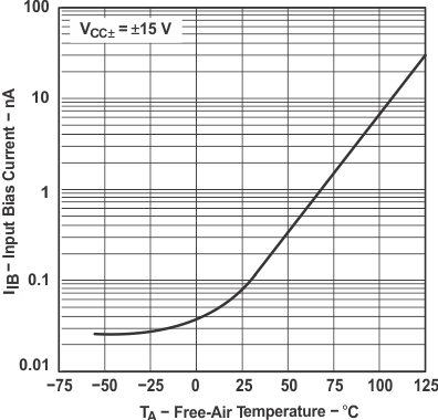
 Figure 1. Input Bias Current vs Free-Air Temperature
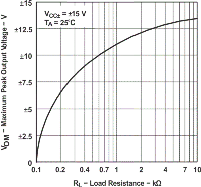
 Figure 3. Maximum Peak Output Voltage vs Load Resistance
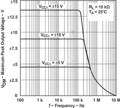
 Figure 2. Maximum Peak Output Voltage vs Frequency
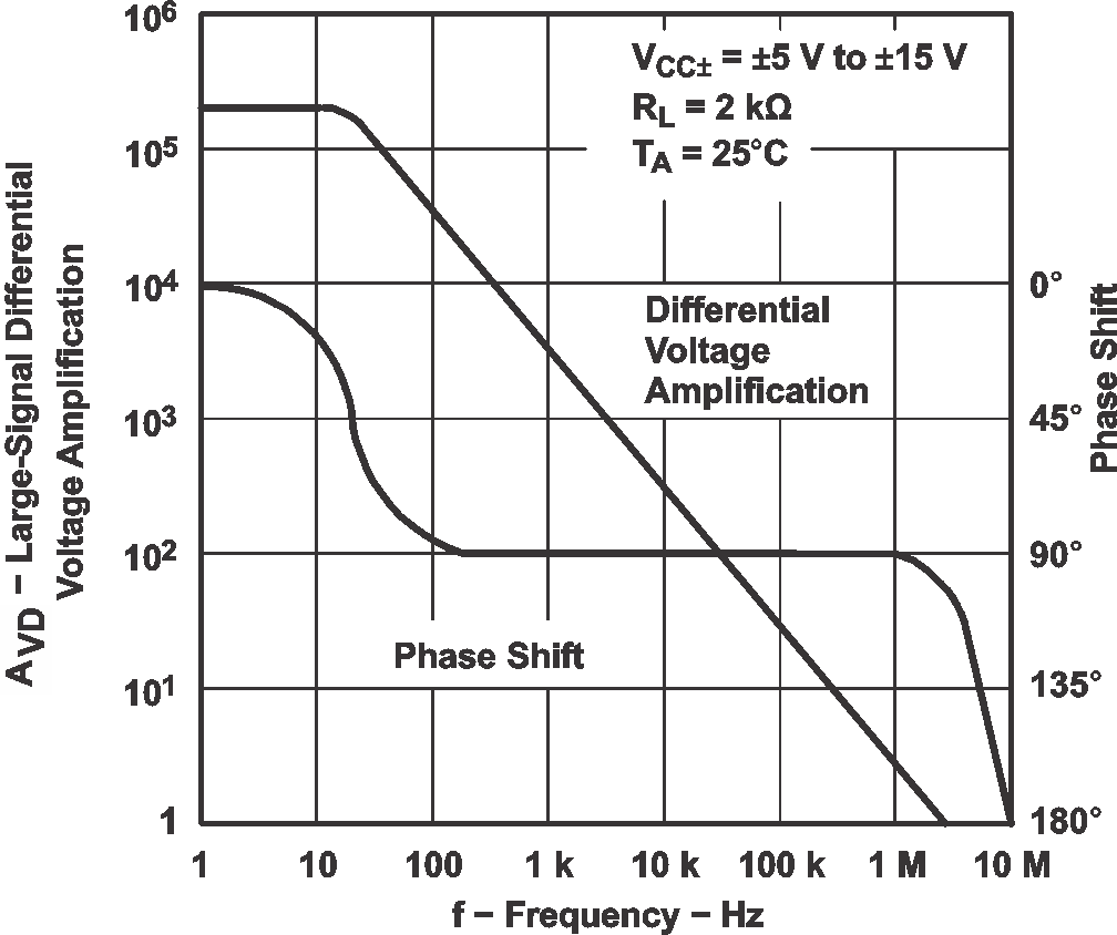
 Figure 4. Large-Signal Differential Voltage Amplification
and Phase Shift vs Frequency