ZHCSD41A DECEMBER 2012 – November 2014 LM10011
PRODUCTION DATA.
10 Layout
10.1 Layout Guidelines
The following guidelines should be followed when designing the PC board for the LM10011:
- Place the LM10011 close to the regulator feedback pin to minimize the FB trace length.
- Place a small capacitor, CVDD, (1 nF) directly adjacent to the VDD and GND pins of the LM10011 to help minimize transients which may occur on the input supply line.
- The high-current path from the board input to the load and the return path should be parallel and close to each other to minimize loop inductance.
- The ground connections for the various components around the LM10011 should be connected directly to each other, and to the LM10011 GND pins, and then connected to the system ground at one point. Do not connect the various component grounds to each other through the high-current ground line.
- For additional information about the operation of the regulator, please consult the respective data sheet and application notes on the respective evaluation boards.
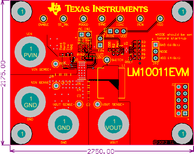
10.2 Layout Example
 Figure 14. Typical Top Layer Layout