SLCS161 June 2017 LM139A-MIL
- 1 Features
- 2 Applications
- 3 Description
- 4 Revision History
- 5 Pin Configuration and Functions
- 6 Specifications
- 7 Detailed Description
- 8 Application and Implementation
- 9 Power Supply Recommendations
- 10Layout
- 11Device and Documentation Support
- 12Mechanical, Packaging, and Orderable Information
封装选项
机械数据 (封装 | 引脚)
散热焊盘机械数据 (封装 | 引脚)
订购信息
7 Detailed Description
7.1 Overview
The LM139A-MIL is a quad comparator with the ability to operate up to an absolute maximum of 36 V on the supply pin. This standard device has proven ubiquity and versatility across a wide range of applications. This is due to very wide supply voltages range (2 V up to 32 V), low Iq, and fast response of the device.
The open-drain output allows the user to configure the output logic low voltage (VOL) and allows the comparator to be used in AND functionality.
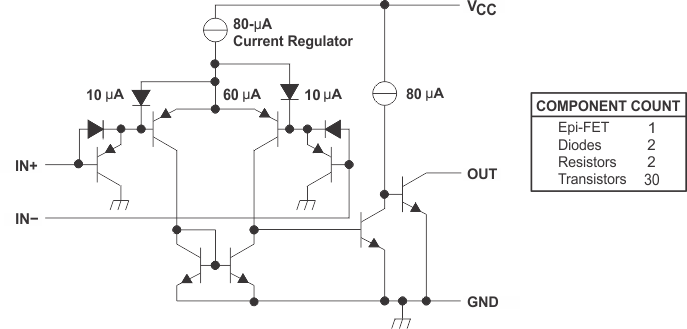
7.2 Functional Block Diagram
 Figure 6. Schematic (Each Comparator)
7.3 Feature Description
The comparator consists of a PNP Darlington pair input, allowing the device to operate with very high gain and fast response with minimal input bias current. The input Darlington pair creates a limit on the input common-mode voltage capability, allowing the comparator to accurately function from ground to (VCC – 1.5 V) differential input. Allow for (VCC – 2 V) at cold temperature.
The output consists of an open-collector NPN (pulldown or low-side) transistor. The output NPN sinks current when the negative input voltage is higher than the positive input voltage and the offset voltage. The VOL is resistive and scales with the output current. See the Specifications section for VOL values with respect to the output current.
7.4 Device Functional Modes
7.4.1 Voltage Comparison
The comparator operates solely as a voltage comparator, comparing the differential voltage between the positive and negative pins and outputting a logic low or high impedance (logic high with pullup) based on the input differential polarity.