ZHCSCX2E January   2014  – October 2017 LM15851

PRODUCTION DATA.  

  1. 特性
  2. 应用
  3. 说明
    1.     Device Images
      1. 16 倍抽取率 — 频谱响应 ƒS = 4GHz,FIN = 1897MHz(–1dBFS 时),ƒ(NCO_x) = 1827MHz
  4. 修订历史记录
  5. Pin Configuration and Functions
    1.     Pin Functions
  6. Specifications
    1. 6.1 Absolute Maximum Ratings
    2. 6.2 ESD Ratings
    3. 6.3 Recommended Operating Conditions
    4. 6.4 Thermal Information
    5. 6.5 Electrical Characteristics
    6. 6.6 Timing Requirements
    7. 6.7 Internal Characteristics
    8. 6.8 Switching Characteristics
    9. 6.9 Typical Characteristics
  7. Detailed Description
    1. 7.1 Overview
    2. 7.2 Functional Block Diagram
    3. 7.3 Feature Description
      1. 7.3.1 Signal Acquisition
      2. 7.3.2 The Analog Inputs
        1. 7.3.2.1 Input Clamp
        2. 7.3.2.2 AC Coupled Input Usage
        3. 7.3.2.3 DC Coupled Input Usage
        4. 7.3.2.4 Handling Single-Ended Input Signals
      3. 7.3.3 Clocking
      4. 7.3.4 Over-Range Function
      5. 7.3.5 ADC Core Features
        1. 7.3.5.1 The Reference Voltage
        2. 7.3.5.2 Common-Mode Voltage Generation
        3. 7.3.5.3 Bias Current Generation
        4. 7.3.5.4 Full Scale Range Adjust
        5. 7.3.5.5 Offset Adjust
        6. 7.3.5.6 Power-Down
        7. 7.3.5.7 Built-In Temperature Monitor Diode
      6. 7.3.6 Digital Down Converter (DDC)
        1. 7.3.6.1 NCO/Mixer
        2. 7.3.6.2 NCO Settings
          1. 7.3.6.2.1 NCO Frequency Phase Selection
          2. 7.3.6.2.2 NCO_0, NCO_1, and NCO_2 (NCO_x)
          3. 7.3.6.2.3 NCO_SEL Bits (2:0)
          4. 7.3.6.2.4 NCO Frequency Setting (Eight Total)
            1. 7.3.6.2.4.1 Basic NCO Frequency-Setting Mode
            2. 7.3.6.2.4.2 Rational NCO Frequency Setting Mode
          5. 7.3.6.2.5 NCO Phase-Offset Setting (Eight Total)
          6. 7.3.6.2.6 Programmable DDC Delay
        3. 7.3.6.3 Decimation Filters
        4. 7.3.6.4 DDC Output Data
        5. 7.3.6.5 Decimation Settings
          1. 7.3.6.5.1 Decimation Factor
          2. 7.3.6.5.2 DDC Gain Boost
      7. 7.3.7 Data Outputs
        1. 7.3.7.1 The Digital Outputs
        2. 7.3.7.2 JESD204B Interface Features and Settings
          1. 7.3.7.2.1  Scrambler Enable
          2. 7.3.7.2.2  Frames Per Multi-Frame (K-1)
          3. 7.3.7.2.3  DDR
          4. 7.3.7.2.4  JESD Enable
          5. 7.3.7.2.5  JESD Test Modes
          6. 7.3.7.2.6  Configurable Pre-Emphasis
          7. 7.3.7.2.7  Serial Output-Data Formatting
          8. 7.3.7.2.8  JESD204B Synchronization Features
          9. 7.3.7.2.9  SYSREF
          10. 7.3.7.2.10 SYNC~
          11. 7.3.7.2.11 Code-Group Synchronization
          12. 7.3.7.2.12 Multiple ADC Synchronization
    4. 7.4 Device Functional Modes
      1. 7.4.1 DDC Modes
      2. 7.4.2 Calibration
        1. 7.4.2.1 Foreground Calibration Mode
        2. 7.4.2.2 Background Calibration Mode
      3. 7.4.3 Timing Calibration Mode
      4. 7.4.4 Test-Pattern Modes
        1. 7.4.4.1 Serializer Test-Mode Details
        2. 7.4.4.2 PRBS Test Modes
        3. 7.4.4.3 Ramp Test Mode
        4. 7.4.4.4 Short and Long-Transport Test Mode
        5. 7.4.4.5 D21.5 Test Mode
        6. 7.4.4.6 K28.5 Test Mode
        7. 7.4.4.7 Repeated ILA Test Mode
        8. 7.4.4.8 Modified RPAT Test Mode
    5. 7.5 Programming
      1. 7.5.1 Using the Serial Interface
        1. 7.5.1.1 Streaming Mode
    6. 7.6 Register Map
      1. 7.6.1 Memory Map
      2. 7.6.2 Register Descriptions
        1. 7.6.2.1 Standard SPI-3.0 (0x000 to 0x00F)
          1. Table 34. Standard SPI-3.0 Registers
          2. 7.6.2.1.1  Configuration A Register (address = 0x000) [reset = 0x3C]
            1. Table 35. CFGA Field Descriptions
          3. 7.6.2.1.2  Configuration B Register (address = 0x001) [reset = 0x00]
            1. Table 36. CFGB Field Descriptions
          4. 7.6.2.1.3  Device Configuration Register (address = 0x002) [reset = 0x00]
            1. Table 37. DEVCFG Field Descriptions
          5. 7.6.2.1.4  Chip Type Register (address = 0x003) [reset = 0x03]
            1. Table 38. CHIP_TYPE Field Descriptions
          6. 7.6.2.1.5  Chip Version Register (address = 0x006) [reset = 0x13]
            1. Table 39. CHIP_VERSION Field Descriptions
          7. 7.6.2.1.6  Vendor Identification Register (address = 0x00C to 0x00D) [reset = 0x0451]
            1. Table 40. VENDOR_ID Field Descriptions
        2. 7.6.2.2 User SPI Configuration (0x010 to 0x01F)
          1. 7.6.2.2.1 User SPI Configuration Register (address = 0x010) [reset = 0x00]
            1. Table 42. USR0 Field Descriptions
        3. 7.6.2.3 General Analog, Bias, Band Gap, and Track and Hold (0x020 to 0x02F)
          1. 7.6.2.3.1 Power-On Reset Register (address = 0x021) [reset = 0x00]
            1. Table 44. POR Field Descriptions
          2. 7.6.2.3.2 I/O Gain 0 Register (address = 0x022) [reset = 0x40]
            1. Table 45. IO_GAIN_0 Field Descriptions
          3. 7.6.2.3.3 IO_GAIN_1 Register (address = 0x023) [reset = 0x00]
            1. Table 46. IO_GAIN_1 Field Descriptions
          4. 7.6.2.3.4 I/O Offset 0 Register (address = 0x025) [reset = 0x40]
            1. Table 47. IO_OFFSET_0 Field Descriptions
          5. 7.6.2.3.5 I/O Offset 1 Register (address = 0x026) [reset = 0x00]
            1. Table 48. IO_OFFSET_1 Field Descriptions
        4. 7.6.2.4 Clock (0x030 to 0x03F)
          1. 7.6.2.4.1 Clock Generator Control 0 Register (address = 0x030) [reset = 0xC0]
            1. Table 50. CLKGEN_0 Field Descriptions
          2. 7.6.2.4.2 Clock Generator Status Register (address = 0x031) [reset = 0x07]
            1. Table 51. CLKGEN_1 Field Descriptions
          3. 7.6.2.4.3 Clock Generator Control 2 Register (address = 0x032) [reset = 0x80]
            1. Table 52. CLKGEN_2 Field Descriptions
          4. 7.6.2.4.4 Analog Miscellaneous Register (address = 0x033) [reset = 0xC3]
            1. Table 53. ANA_MISC Field Descriptions
          5. 7.6.2.4.5 Input Clamp Enable Register (address = 0x034) [reset = 0x2F]
            1. Table 54. IN_CL_EN Field Descriptions
        5. 7.6.2.5 Serializer (0x040 to 0x04F)
          1. 7.6.2.5.1 Serializer Configuration Register (address = 0x040) [reset = 0x04]
            1. Table 56. SER_CFG Field Descriptions
        6. 7.6.2.6 ADC Calibration (0x050 to 0x1FF)
          1. 7.6.2.6.1 Calibration Configuration 0 Register (address = 0x050) [reset = 0x06]
            1. Table 58. CAL_CFG0 Field Descriptions
          2. 7.6.2.6.2 Calibration Configuration 1 Register (address = 0x051) [reset = 0xF4]
            1. Table 59. CAL_CFG1 Field Descriptions
          3. 7.6.2.6.3 Calibration Background Control Register (address = 0x057) [reset = 0x10]
            1. Table 60. CAL_BACK Field Descriptions
          4. 7.6.2.6.4 ADC Pattern and Over-Range Enable Register (address = 0x058) [reset = 0x00]
            1. Table 61. ADC_PAT_OVR_EN Field Descriptions
          5. 7.6.2.6.5 Calibration Vectors Register (address = 0x05A) [reset = 0x00]
            1. Table 62. CAL_VECTOR Field Descriptions
          6. 7.6.2.6.6 Calibration Status Register (address = 0x05B) [reset = undefined]
            1. Table 63. CAL_STAT Field Descriptions
          7. 7.6.2.6.7 Timing Calibration Register (address = 0x066) [reset = 0x02]
            1. Table 64. CAL_STAT Field Descriptions
        7. 7.6.2.7 Digital Down Converter and JESD204B (0x200-0x27F)
          1. 7.6.2.7.1  Digital Down-Converter (DDC) Control Register (address = 0x200) [reset = 0x10]
            1. Table 66. DDC_CTRL1 Field Descriptions
          2. 7.6.2.7.2  JESD204B Control 1 Register (address = 0x201) [reset = 0x0F]
            1. Table 67. JESD_CTRL1 Field Descriptions
          3. 7.6.2.7.3  JESD204B Control 2 Register (address = 0x202) [reset = 0x00]
            1. Table 68. JESD_CTRL2 Field Descriptions
          4. 7.6.2.7.4  JESD204B Device ID (DID) Register (address = 0x203) [reset = 0x00]
            1. Table 69. JESD_DID Field Descriptions
          5. 7.6.2.7.5  JESD204B Control 3 Register (address = 0x204) [reset = 0x00]
            1. Table 70. JESD_CTRL3 Field Descriptions
          6. 7.6.2.7.6  JESD204B and System Status Register (address = 0x205) [reset = Undefined]
            1. Table 71. JESD_STATUS Field Descriptions
          7. 7.6.2.7.7  Overrange Threshold 0 Register (address = 0x206) [reset = 0xF2]
            1. Table 72. OVR_T0 Field Descriptions
          8. 7.6.2.7.8  Overrange Threshold 1 Register (address = 0x207) [reset = 0xAB]
            1. Table 73. OVR_T1 Field Descriptions
          9. 7.6.2.7.9  Overrange Period Register (address = 0x208) [reset = 0x00]
            1. Table 74. OVR_N Field Descriptions
          10. 7.6.2.7.10 DDC Configuration Preset Mode Register (address = 0x20C) [reset = 0x00]
            1. Table 75. NCO_MODE Field Descriptions
          11. 7.6.2.7.11 DDC Configuration Preset Select Register (address = 0x20D) [reset = 0x00]
            1. Table 76. NCO_SEL Field Descriptions
          12. 7.6.2.7.12 Rational NCO Reference Divisor Register (address = 0x20E to 0x20F) [reset = 0x0000]
            1. Table 77. NCO_RDIV Field Descriptions
          13. 7.6.2.7.13 NCO Frequency (Preset x) Register (address = see ) [reset = see ]
            1. Table 78. NCO_FREQ_x Field Descriptions
          14. 7.6.2.7.14 NCO Phase (Preset x) Register (address = see ) [reset = see ]
            1. Table 79. NCO_PHASE_x Field Descriptions
          15. 7.6.2.7.15 DDC Delay (Preset x) Register (address = see ) [reset = see ]
            1. Table 80. DDC_DLY_x Field Descriptions
  8. Application and Implementation
    1. 8.1 Application Information
    2. 8.2 Typical Application
      1. 8.2.1 RF Sampling Receiver
        1. 8.2.1.1 Design Requirements
        2. 8.2.1.2 Detailed Design Procedure
        3. 8.2.1.3 Application Curves
    3. 8.3 Initialization Set-Up
      1. 8.3.1 JESD204B Startup Sequence
    4. 8.4 Dos and Don'ts
      1. 8.4.1 Common Application Pitfalls
  9. Power Supply Recommendations
    1. 9.1 Supply Voltage
  10. 10Layout
    1. 10.1 Layout Guidelines
    2. 10.2 Layout Example
    3. 10.3 Thermal Management
  11. 11器件和文档支持
    1. 11.1 器件支持
      1. 11.1.1 Third-Party Products Disclaimer
      2. 11.1.2 开发支持
      3. 11.1.3 器件命名规则
    2. 11.2 文档支持
      1. 11.2.1 相关文档
    3. 11.3 社区资源
    4. 11.4 商标
    5. 11.5 静电放电警告
    6. 11.6 Glossary
  12. 12机械、封装和可订购信息

封装选项

机械数据 (封装 | 引脚)
散热焊盘机械数据 (封装 | 引脚)
订购信息

Typical Characteristics

Unless otherwise noted, these specifications apply for V(VA12) = V(VD12) = 1.2 V, V(VA19) = 1.9 V, VIN FSR (AC coupled) = Default setting, differential AC-coupled sinewave input clock, ƒ(DEVCLK) = 4 GHz at 0.5 VPP with 50% duty cycle, R(RBIAS) = 3.3 kΩ ±0.1%, after a Foreground mode calibration with Timing Calibration enabled. TA = 25°C. VI = –1 dBFS.
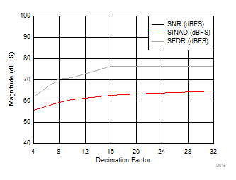
LM15851 D019_SLAS989.gif
FIN = 608 MHz
Figure 3. SNR, SINAD, SFDR vs Decimation Setting
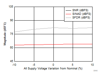
LM15851 D043_SLAS989.gif
Decimate by 16 mode FIN = 608 MHz
Figure 5. SNR, SINAD, SFDR vs Supply
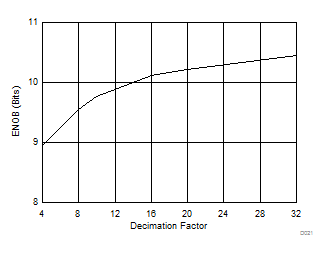
LM15851 D021_SLAS989.gif
FIN = 608 MHz
Figure 7. ENOB vs Decimation Setting
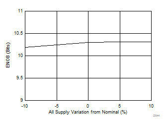
LM15851 D044_SLAS989.gif
Decimate by 16 mode FIN = 608 MHz
Figure 9. ENOB vs Supply
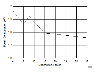
LM15851 D022_SLAS989.gif
FIN = 608 MHz
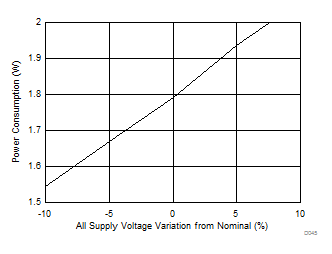
Figure 11. Power Consumption vs Decimation Setting
LM15851 D045_SLAS989.gif
Decimate by 16 mode FIN = 608 MHz
Figure 13. Power Consumption vs Supply
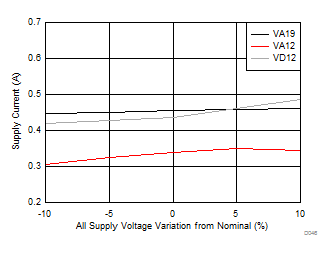
LM15851 D046_SLAS989.gif
Decimate by 16 mode FIN = 608 MHz
Figure 15. Supply Current vs Supply Voltage
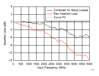
LM15851 D037_SLAS989.gif
Foreground calibration mode
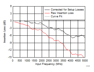
Figure 17. Insertion Loss vs Input Frequency
LM15851 D055_SLAS989.gif
Figure 19. Decimate by 4 - Stopband Response
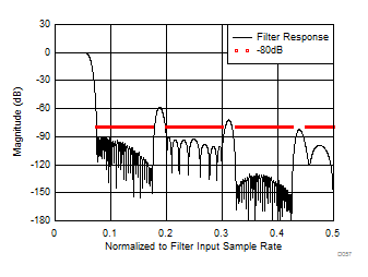
LM15851 D057_SLAS989.gif
Figure 21. Decimate by 8 - Stopband Response
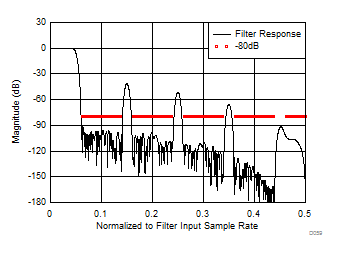
LM15851 D059_SLAS989.gif
Figure 23. Decimate by 10 - Stopband Response
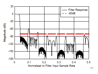
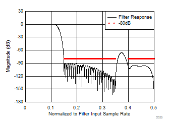
LM15851 D061_SLAS989.gif
Figure 25. Decimate by 16 - Stopband Response
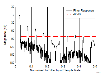
LM15851 D063_SLAS989.gif
Figure 27. Decimate by 20 - Stopband Response
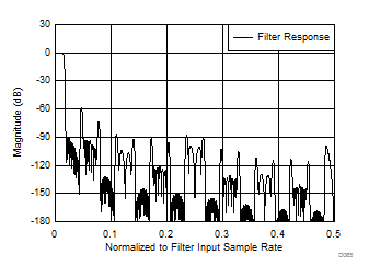
LM15851 D065_SLAS989.gif
Figure 29. Decimate by 32 - Stopband Response
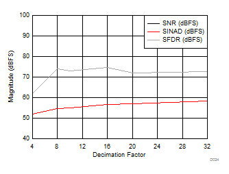
LM15851 D024_SLAS989.gif
FIN = 2483 MHz
Figure 4. SNR, SINAD, SFDR vs Decimation Setting
LM15851 D033_SLAS989.gif
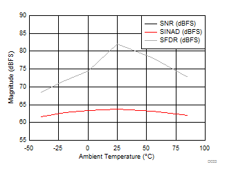
Decimate by 16 mode FIN = 608 MHz
Figure 6. SNR, SINAD, SFDR vs Temperature
LM15851 D026_SLAS989.gif
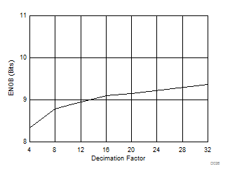
FIN = 2483 MHz
Figure 8. ENOB vs Decimation Setting
LM15851 D034_SLAS989.gif
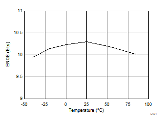
Decimate by 16 mode FIN = 608 MHz
Figure 10. ENOB vs Temperature
LM15851 D035_SLAS989.gif
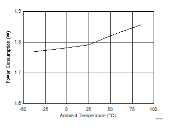
Decimate by 16 mode FIN = 608 MHz
Figure 12. Power Consumption vs Temperature
LM15851 D023_SLAS989.gif
FIN = 608 MHz
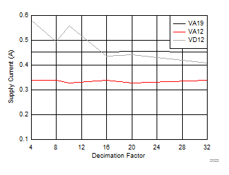
Figure 14. Supply Current vs Decimation Setting
LM15851 D036_SLAS989.gif
Decimate by 16 mode FIN = 608 MHz
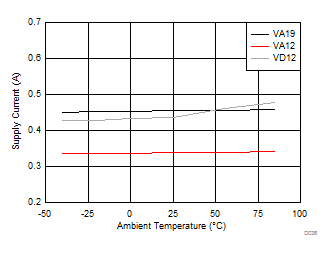
Figure 16. Supply Current vs Temperature
LM15851 D038_SLAS989.gif
Background calibration mode
Figure 18. Insertion Loss vs Input Frequency
LM15851 D056_SLAS989.gif
Figure 20. Decimate by 4 - Passband Response
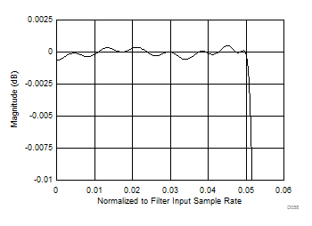
LM15851 D058_SLAS989.gif
Figure 22. Decimate by 8 - Passband Response
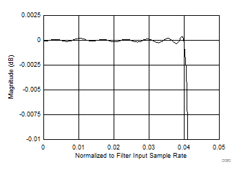
LM15851 D060_SLAS989.gif
Figure 24. Decimate by 10 - Passband Response
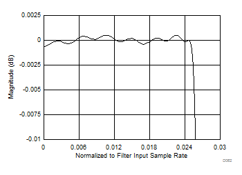
LM15851 D062_SLAS989.gif
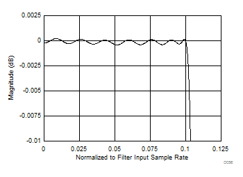
Figure 26. Decimate by 16 - Passband Response
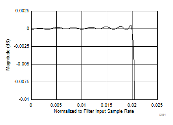
LM15851 D064_SLAS989.gif
Figure 28. Decimate by 20 - Passband Response
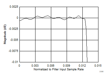
LM15851 D066_SLAS989.gif
Figure 30. Decimate by 32 - Passband Response