ZHCS541M September 2008 – November 2014 LM22672 , LM22672-Q1
PRODUCTION DATA.
- 1 特性
- 2 应用
- 3 说明
- 4 修订历史记录
- 5 Pin Configuration and Functions
- 6 Specifications
- 7 Detailed Description
- 8 Application and Implementation
- 9 Power Supply Recommendations
- 10Layout
- 11器件和文档支持
- 12机械、封装和可订购信息
10 Layout
10.1 Layout Guidelines
Board layout is critical for the proper operation of switching power supplies. First, the ground plane area must be sufficient for thermal dissipation purposes. Second, appropriate guidelines must be followed to reduce the effects of switching noise. Switch mode converters are very fast switching devices. In such cases, the rapid increase of input current combined with the parasitic trace inductance generates unwanted L di/dt noise spikes. The magnitude of this noise tends to increase as the output current increases. This noise may turn into electromagnetic interference (EMI) and can also cause problems in device performance. Therefore, care must be taken in layout to minimize the effect of this switching noise.
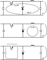
The most important layout rule is to keep the ac current loops as small as possible. Figure 23 shows the current flow in a buck converter. The top schematic shows a dotted line which represents the current flow during the FET switch on-state. The middle schematic shows the current flow during the FET switch off-state.
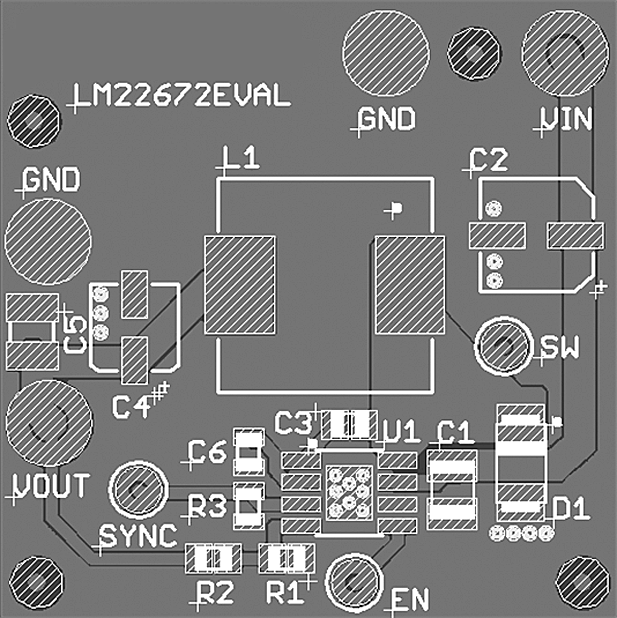
The bottom schematic shows the currents referred to as ac currents. These ac currents are the most critical because they are changing in a very short time period. The dotted lines of the bottom schematic are the traces to keep as short and wide as possible. This will also yield a small loop area reducing the loop inductance. To avoid functional problems due to layout, review the PCB layout example. Best results are achieved if the placement of the LM22672 device, the bypass capacitor, the Schottky diode, RFBB, RFBT, and the inductor are placed as shown in the example. Note that, in the layout shown, R1 = RFBB and R2 = RFBT. It is also recommended to use 2 oz copper boards or heavier to help thermal dissipation and to reduce the parasitic inductances of board traces. See application note AN-1229 SIMPLE SWITCHER® PCB Layout Guidelines (SNVA054) for more information.
 Figure 23. Current Flow in a Buck Application
10.2 Layout Example

10.3 Thermal Considerations
The components with the highest power dissipation are the power diode and the power MOSFET internal to the LM22672 regulator. The easiest method to determine the power dissipation within the LM22672 is to measure the total conversion losses then subtract the power losses in the diode and inductor. The total conversion loss is the difference between the input power and the output power. An approximation for the power diode loss is shown in Equation 18:

where
- VD is the diode voltage drop.
An approximation for the inductor power is shown in Equation 19:

Where:
RL is the dc resistance of the inductor.
The 1.1 factor is an approximation for the ac losses.
The regulator has an exposed thermal pad to aid power dissipation. Adding multiple vias under the device to the ground plane will greatly reduce the regulator junction temperature. Selecting a diode with an exposed pad will also aid the power dissipation of the diode. The most significant variables that affect the power dissipation of the regulator are output current, input voltage and operating frequency. The power dissipated while operating near the maximum output current and maximum input voltage can be appreciable. The junction-to-ambient thermal resistance of the LM22672 will vary with the application. The most significant variables are the area of copper in the PC board, the number of vias under the IC exposed pad and the amount of forced air cooling provided. A large continuous ground plane on the top or bottom PCB layer will provide the most effective heat dissipation. The integrity of the solder connection from the IC exposed pad to the PC board is critical. Excessive voids will greatly diminish the thermal dissipation capacity. The junction-to-ambient thermal resistance of the LM22672 SO PowerPAD package is specified in the Electrical Characteristics table. See AN-2020 Thermal Design By Insight, Not Hindsight (SNVA419) for more information.