ZHCS544L September 2008 – November 2014 LM22675 , LM22675-Q1
PRODUCTION DATA.
8 Application and Implementation
NOTE
Information in the following applications sections is not part of the TI component specification, and TI does not warrant its accuracy or completeness. TI’s customers are responsible for determining suitability of components for their purposes. Customers should validate and test their design implementation to confirm system functionality.
8.1 Application Information
The LM22675 device is a step down dc-to-dc regulator. It is typically used to convert a higher dc voltage to a lower dc voltage with a maximum output current of 1 A. Detailed Design Procedure can be used to select components for the LM22675 device. Alternately, the WEBENCH® software may be used to generate complete designs. When generating a design, the WEBENCH® software utilizes iterative design procedure and accesses comprehensive databases of components. Go to WEBENCH Designer for more details. This section presents a simplified discussion of the design process.
8.1.1 Output Voltage Divider Selection
For output voltages between about 1.285 V and 5 V, the -ADJ option should be used, with an appropriate voltage divider as shown in Figure 13. Equation 10 can be used to calculate the resistor values of this divider.

A good value for RFBB is 1 kΩ. This will help to provide some of the minimum load current requirement and reduce susceptibility to noise pick-up. The top of RFBT should be connected directly to the output capacitor or to the load for remote sensing. If the divider is connected to the load, a local high-frequency bypass should be provided at that location.
For output voltages of 5 V, the -5.0 option should be used. In this case no divider is needed and the FB pin is connected to the output. The approximate values of the internal voltage divider are as follows: 7.38 kΩ from the FB pin to the input of the error amplifier and 2.55 kΩ from there to ground.
Both the -ADJ and -5.0 options can be used for output voltages greater than 5 V, by using the correct output divider. As mentioned in Internal Loop Compensation, the -5.0 option is optimized for output voltages of 5 V. However, for output voltages greater than 5 V, this option may provide better loop bandwidth than the -ADJ option, in some applications. If the -5.0 option is to be used at output voltages greater than 5 V, Equation 11 should be used to determine the resistor values in the output divider.

A value of RFBB of about 1 kΩ is a good first choice.
 Figure 13. Resistive Feedback Divider
A maximum value of 10 kΩ is recommended for the sum of RFBB and RFBT to maintain good output voltage accuracy for the -ADJ option. A maximum of 2 kΩ is recommended for the -5.0 option. For the -5.0 option, the total internal divider resistance is typically 9.93 kΩ.
In all cases the output voltage divider should be placed as close as possible to the FB pin of the LM22675, because this is a high impedance input and is susceptible to noise pick-up.
8.1.2 Power Diode
A Schottky-type power diode is required for all LM22675 applications. Ultra-fast diodes are not recommended and may result in damage to the IC due to reverse recovery current transients. The near ideal reverse recovery characteristics and low forward voltage drop of Schottky diodes are particularly important for high input voltage and low output voltage applications common to the LM22675. The reverse breakdown rating of the diode should be selected for the maximum VIN, plus some safety margin. A good rule of thumb is to select a diode with a reverse voltage rating of 1.3 times the maximum input voltage.
Select a diode with an average current rating at least equal to the maximum load current that will be seen in the application.
8.2 Typical Application
8.2.1 Typical Buck Regulator Application
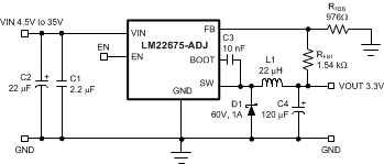
Figure 14 shows an example of converting an input voltage range of 5.5 V to 42 V, to an output of 3.3 V at 1 A.
 Figure 14. Typical Buck Regulator Application
8.2.1.1 Design Requirements
| DESIGN PARAMETERS | EXAMPLE VALUE |
|---|---|
| Driver Supply Voltage (VIN) | 4.5 to 42 V |
| Output Voltage (VOUT) | 3.3 V |
| RFBT | Calculated based on RFBB and VREF of 1.285 V. |
| RFBB | 1 kΩ to 10 kΩ |
| IOUT | 1 A |
8.2.1.2 Detailed Design Procedure
8.2.1.2.1 External Components
The following guidelines should be used when designing a step-down (buck) converter with the LM22675.
8.2.1.2.2 Inductor
The inductor value is determined based on the load current, ripple current, and the minimum and maximum input voltages. To keep the application in continuous conduction mode (CCM), the maximum ripple current, IRIPPLE, should be less than twice the minimum load current. The general rule of keeping the inductor current peak-to-peak ripple around 30% of the nominal output current is a good compromise between excessive output voltage ripple and excessive component size and cost. Using this value of ripple current, the value of inductor, L, is calculated using Equation 12.

Where:
Fsw is the switching frequency.
Vin should be taken at its maximum value, for the given application.
The formula in Equation 12 provides a guide to select the value of the inductor L; the nearest standard value will then be used in the circuit.
Once the inductor is selected, the actual ripple current can be found from Equation 13.

Increasing the inductance will generally slow down the transient response but reduce the output voltage ripple. Reducing the inductance will generally improve the transient response but increase the output voltage ripple.
The inductor must be rated for the peak current, IPK, in a given application, to prevent saturation. During normal loading conditions, the peak current is equal to the load current plus 1/2 of the inductor ripple current.
During an overload condition, as well as during certain load transients, the controller may trip current limit. In this case the peak inductor current is given by ICL, found in the Electrical Characteristics table. Good design practice requires that the inductor rating be adequate for this overload condition.
NOTE
If the inductor is not rated for the maximum expected current, it can saturate resulting in damage to the LM22675 and/or the power diode.
8.2.1.2.3 Input Capacitor
The input capacitor selection is based on both input voltage ripple and RMS current. Good quality input capacitors are necessary to limit the ripple voltage at the VIN pin while supplying most of the regulator current during switch on-time. Low ESR ceramic capacitors are preferred. Larger values of input capacitance are desirable to reduce voltage ripple and noise on the input supply. This noise may find its way into other circuitry, sharing the same input supply, unless adequate bypassing is provided. A very approximate formula for determining the input voltage ripple is shown in Equation 14.

Where:
Vri is the peak-to-peak ripple voltage at the switching frequency.
Another concern is the RMS current passing through this capacitor. Equation 15 gives an approximation to this current.

The capacitor must be rated for at least this level of RMS current at the switching frequency.
All ceramic capacitors have large voltage coefficients, in addition to normal tolerances and temperature coefficients. To help mitigate these effects, multiple capacitors can be used in parallel to bring the minimum capacitance up to the desired value. This may also help with RMS current constraints by sharing the current among several capacitors. Many times it is desirable to use an electrolytic capacitor on the input, in parallel with the ceramics. The moderate ESR of this capacitor can help to damp any ringing on the input supply caused by long power leads. This method can also help to reduce voltage spikes that may exceed the maximum input voltage rating of the LM22675.
It is good practice to include a high frequency bypass capacitor as close as possible to the LM22675. This small case size, low ESR, ceramic capacitor should be connected directly to the VIN and GND pins with the shortest possible PCB traces. Values in the range of 0.47 µF to 1 µF are appropriate. This capacitor helps to provide a low impedance supply to sensitive internal circuitry. It also helps to suppress any fast noise spikes on the input supply that may lead to increased EMI.
8.2.1.2.4 Output Capacitor
The output capacitor is responsible for filtering the output voltage and supplying load current during transients. Capacitor selection depends on application conditions as well as ripple and transient requirements. Best performance is achieved with a parallel combination of ceramic capacitors and a low ESR SP™ or POSCAP™ type. Very low ESR capacitors such as ceramics reduce the output ripple and noise spikes, while higher value electrolytics or polymer provide large bulk capacitance to supply transients. Assuming very low ESR, Equation 16 gives an approximation to the output voltage ripple.

Typically, a total value of 100 µF, or greater, is recommended for output capacitance.
In applications with Vout less than 3.3 V, it is critical that low ESR output capacitors are selected. This will limit potential output voltage overshoots as the input voltage falls below the device normal operating range.
8.2.1.2.5 Boot-Strap Capacitor
The bootstrap capacitor between the BOOT pin and the SW pin supplies the gate current to turn on the N-channel MOSFET. The recommended value of this capacitor is 10 nF and should be a good quality, low ESR ceramic capacitor. In some cases it may be desirable to slow down the turn-on of the internal power MOSFET, in order to reduce EMI. This can be done by placing a small resistor in series with the Cboot capacitor. Resistors in the range of 10 Ω to 50 Ω can be used. This technique should only be used when absolutely necessary, because it will increase switching losses and thereby reduce efficiency.
8.2.1.3 Application Curves
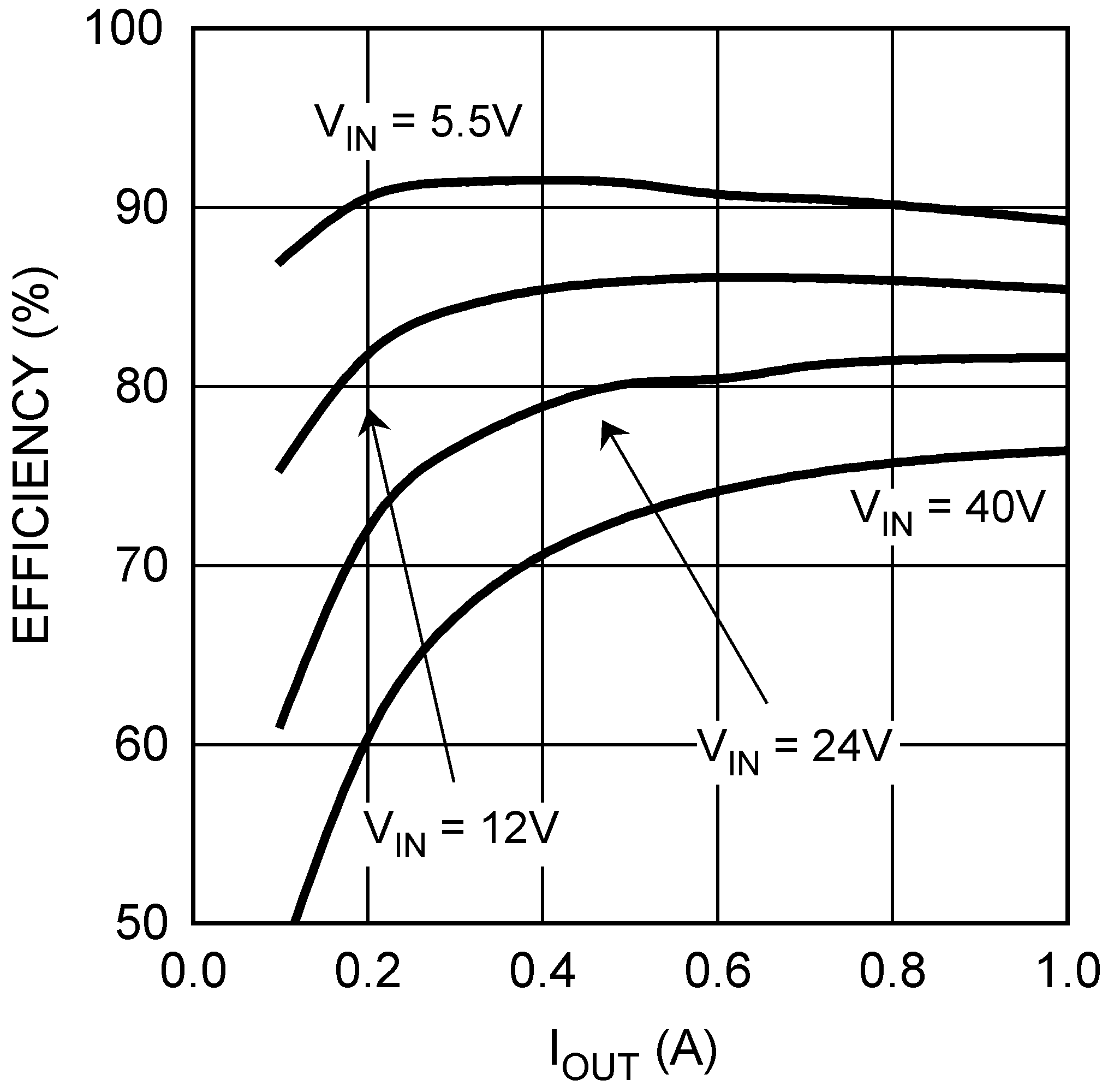
 Figure 15. Efficiency vs IOUT and VIN, VOUT = 3.3 V
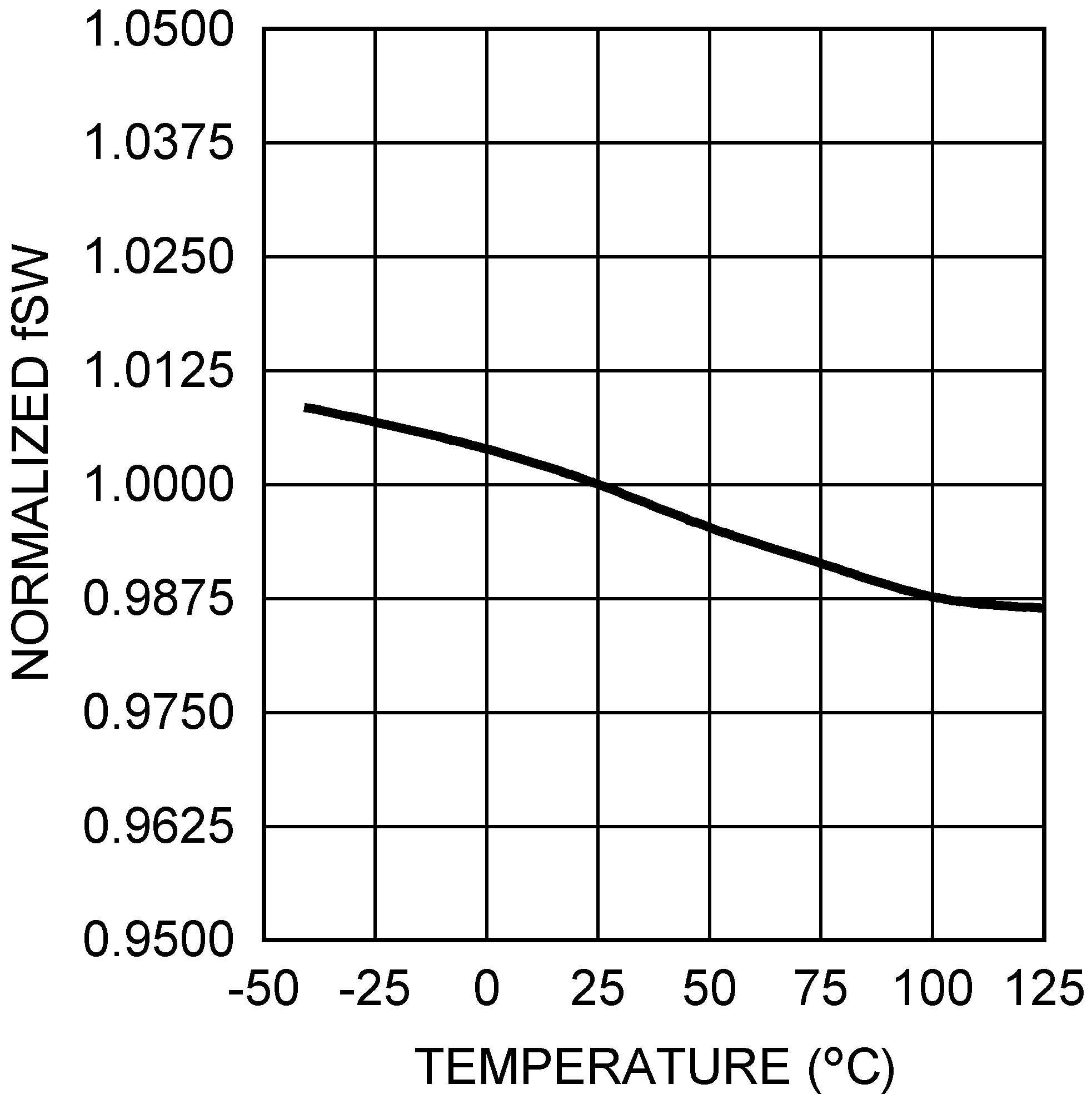
 Figure 16. Normalized Switching Frequency vs Temperature