ZHCS540L September   2008  – November 2014 LM22676 , LM22676-Q1

PRODUCTION DATA.  

  1. 特性
  2. 应用
  3. 说明
  4. 修订历史记录
  5. Pin Configuration and Functions
  6. Specifications
    1. 6.1 Absolute Maximum Ratings
    2. 6.2 Handling Ratings: LM22676
    3. 6.3 Handling Ratings: LM22676-Q1
    4. 6.4 Recommended Operating Conditions
    5. 6.5 Thermal Information
    6. 6.6 Electrical Characteristics
    7. 6.7 Typical Characteristics
  7. Detailed Description
    1. 7.1 Overview
    2. 7.2 Functional Block Diagram
    3. 7.3 Feature Description
      1. 7.3.1 Precision Enable and UVLO
      2. 7.3.2 Soft-Start
      3. 7.3.3 Boot-Strap Supply
      4. 7.3.4 Internal Compensation
    4. 7.4 Device Functional Modes
      1. 7.4.1 Current Limit
      2. 7.4.2 Thermal Protection
      3. 7.4.3 Duty-Cycle Limits
  8. Application and Implementation
    1. 8.1 Application Information
      1. 8.1.1 Output Voltage Divider Selection
      2. 8.1.2 Power Diode
    2. 8.2 Typical Application
      1. 8.2.1 Typical Buck Regulator Application
        1. 8.2.1.1 Design Requirements
        2. 8.2.1.2 Detailed Design Procedure
          1. 8.2.1.2.1 External Components
          2. 8.2.1.2.2 Inductor
          3. 8.2.1.2.3 Input Capacitor
          4. 8.2.1.2.4 Output Capacitor
          5. 8.2.1.2.5 Boot-Strap Capacitor
        3. 8.2.1.3 Application Curves
  9. Power Supply Recommendations
  10. 10Layout
    1. 10.1 Layout Guidelines
    2. 10.2 Layout Examples
    3. 10.3 Thermal Considerations
  11. 11器件和文档支持
    1. 11.1 文档支持
      1. 11.1.1 相关文档 
    2. 11.2 相关链接
    3. 11.3 商标
    4. 11.4 静电放电警告
    5. 11.5 术语表
  12. 12机械、封装和可订购信息

封装选项

机械数据 (封装 | 引脚)
散热焊盘机械数据 (封装 | 引脚)
订购信息

5 Pin Configuration and Functions

SO PowerPAD Package
8-Pin
Top View
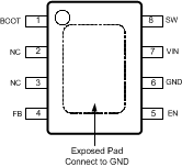
LM22676 LM22676-Q1 30076540.gif
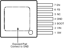
PFM Package
8-Pin
Top View
LM22676 LM22676-Q1 30076502.gif

Pin Functions

PIN TYPE DESCRIPTION APPLICATION INFORMATION
NAME SO
PowerPAD
PFM
BOOT 1 3 I Bootstrap input Provides the gate voltage for the high side N-FET.
NC 2, 3 5 Not Connected Pins are not electrically connected inside the chip. Pins do function as thermal conductor.
FB 4 6 I Feedback pin Feedback input to regulator.
EN 5 7 I Enable input Used to control regulator start-up and shutdown. See Precision Enable and UVLO section of data sheet.
GND 6 4 Ground input to regulator;
system common
System ground pin.
VIN 7 2 I Input Voltage Input supply to regulator
SW 8 1 O Switch pin Switching output of regulator
EP EP EP Exposed Pad Connect to ground. Provides thermal connection to PCB. See Thermal Considerations.