SLVS047L November   1981  – January 2015 LM237 , LM337

PRODUCTION DATA.  

  1. Features
  2. Applications
  3. Description
  4. Simplified Schematic
  5. Revision History
  6. Pin Configuration and Functions
  7. Specifications
    1. 7.1 Absolute Maximum Ratings
    2. 7.2 ESD Ratings
    3. 7.3 Recommended Operating Conditions
    4. 7.4 Thermal Information
    5. 7.5 Electrical Characteristics
    6. 7.6 Electrical Characteristics
    7. 7.7 Typical Characteristics
  8. Detailed Description
    1. 8.1 Overview
    2. 8.2 Functional Block Diagram
    3. 8.3 Design Schematic
    4. 8.4 Feature Description
      1. 8.4.1 Output Voltage Adjustment
    5. 8.5 Device Functional Modes
      1. 8.5.1 Adjustable Output Mode
  9. Application and Implementation
    1. 9.1 Application Information
      1. 9.1.1 General Configurations
    2. 9.2 Typical Application
      1. 9.2.1 Design Requirements
      2. 9.2.2 Detailed Design Procedure
      3. 9.2.3 Application Curves
  10. 10Power Supply Recommendations
  11. 11Layout
    1. 11.1 Layout Guidelines
    2. 11.2 Layout Example
  12. 12Device and Documentation Support
    1. 12.1 Related Links
    2. 12.2 Trademarks
    3. 12.3 Electrostatic Discharge Caution
    4. 12.4 Glossary
  13. 13Mechanical, Packaging, and Orderable Information

封装选项

机械数据 (封装 | 引脚)
散热焊盘机械数据 (封装 | 引脚)
订购信息

11 Layout

11.1 Layout Guidelines

Traces on the input and output pins should be thick enough to carry 1.5 A of current without violating thermal requirements of the device or the system. In addition, a 1-µF solid tantalum capacitor is required on the input pin if the regulator is more than 10 cm from the power supply filter capacitor. A 1-µF solid tantalum or 10-µF aluminum electrolytic capacitor is required on the output pin for stability.

11.2 Layout Example
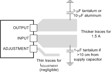
LM237_Layout.gifFigure 5. Layout Diagram