SLVS047L November   1981  – January 2015 LM237 , LM337

PRODUCTION DATA.  

  1. Features
  2. Applications
  3. Description
  4. Simplified Schematic
  5. Revision History
  6. Pin Configuration and Functions
  7. Specifications
    1. 7.1 Absolute Maximum Ratings
    2. 7.2 ESD Ratings
    3. 7.3 Recommended Operating Conditions
    4. 7.4 Thermal Information
    5. 7.5 Electrical Characteristics
    6. 7.6 Electrical Characteristics
    7. 7.7 Typical Characteristics
  8. Detailed Description
    1. 8.1 Overview
    2. 8.2 Functional Block Diagram
    3. 8.3 Design Schematic
    4. 8.4 Feature Description
      1. 8.4.1 Output Voltage Adjustment
    5. 8.5 Device Functional Modes
      1. 8.5.1 Adjustable Output Mode
  9. Application and Implementation
    1. 9.1 Application Information
      1. 9.1.1 General Configurations
    2. 9.2 Typical Application
      1. 9.2.1 Design Requirements
      2. 9.2.2 Detailed Design Procedure
      3. 9.2.3 Application Curves
  10. 10Power Supply Recommendations
  11. 11Layout
    1. 11.1 Layout Guidelines
    2. 11.2 Layout Example
  12. 12Device and Documentation Support
    1. 12.1 Related Links
    2. 12.2 Trademarks
    3. 12.3 Electrostatic Discharge Caution
    4. 12.4 Glossary
  13. 13Mechanical, Packaging, and Orderable Information

封装选项

机械数据 (封装 | 引脚)
散热焊盘机械数据 (封装 | 引脚)
订购信息

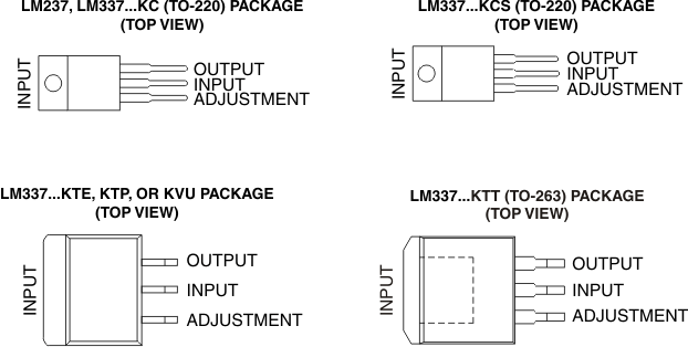
6 Pin Configuration and Functions

po_lvs047.gif

Pin Functions

PIN TYPE DESCRIPTION
NAME NO.
ADJUSTMENT 1 I Adjustment pin for the output voltage. Connect two external resistors to adjust the output voltage.
INPUT 2 I Input voltage. The input voltage and current will be designated VI and II respectively.
OUTPUT 3 O Output voltage. The output voltage and current will be designated VO and IO respectively.