SNVS572E July 2008 – January 2016 LM25037 , LM25037-Q1
PRODUCTION DATA.
- 1 Features
- 2 Applications
- 3 Description
- 4 Revision History
- 5 Pin Configuration and Functions
- 6 Specifications
- 7 Detailed Description
- 8 Application and Implementation
- 9 Power Supply Recommendations
- 10Layout
- 11Device and Documentation Support
- 12Mechanical, Packaging, and Orderable Information
7 Detailed Description
7.1 Overview
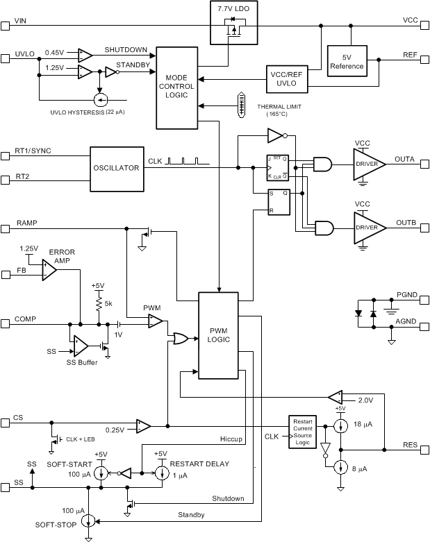
The LM25037 PWM controller contains all the features necessary to implement double-ended power converter topologies such as push-pull, half-bridge and full-bridge. The unique architecture allows the modulator to be configured for either voltage-mode or current-mode control. The LM25037 provides two alternating gate driver outputs to drive the primary side power MOSFETs with programmable forced dead-time. The LM25037 can be configured to operate with bias voltages ranging from 5.5 V to 75 V. Additional features include line undervoltage lockout, cycle-by-cycle current limit, voltage feed-forward compensation, and hiccup mode fault protection with adjustable delays, soft-start, and a 2-MHz capable oscillator with synchronization capability, precision reference, and thermal shutdown. These rich set of features simplify the design of double ended topologies. The functional block diagram is show in the Functional Block Diagram section.
7.2 Functional Block Diagram
7.3 Feature Description
7.3.1 High-Voltage Start-Up Regulator
The LM25037 contains an internal high voltage, low drop-out start-up regulator that allows the input pin (VIN) to be connected directly to the supply voltage over a range of 5.5 V to a maximum of 75 V. The regulator output at VCC (7.7 V) is internally current limited with a specified minimum of 20 mA. When the UVLO pin potential is greater than 0.45 V, the VCC regulator is enabled to charge an external capacitor connected to the VCC pin. The VCC regulator provides power to the voltage reference (REF) and the gate drivers (OUTA and OUTB). When the voltage on the VCC pin exceeds its undervoltage (VCC UV) threshold of 5-V nominal, the internal voltage reference (REF) reaches its regulation set point of 5 V and the UVLO voltage is greater than 1.25 V, the controller outputs are enabled. The value selected for the VCC capacitor depends on the total system design, and its start-up characteristics. The recommended range of values for the VCC capacitor is 0.47 µF to 10 µF. The internal power dissipation of the LM25037 can be reduced by powering VCC from an external supply. In typical applications, an auxiliary transformer winding is connected through a diode to the VCC pin. This winding must raise the VCC voltage above 8.2 V to shut off the internal start-up regulator. Powering VCC from an auxiliary winding improves efficiency while reducing the controller’s power dissipation. The VCC UV circuit will still function in this mode, requiring that VCC never falls below 5-V nominal during the start-up sequence. The VCC regulator series pass transistor includes a diode between VCC and VIN that should not be forward biased in normal operation. Therefore the auxiliary VCC voltage should never exceed the VIN voltage.
An external DC bias voltage can be used instead of the internal regulator by connecting the external bias voltage to both the VCC and the VIN pins. In this particular case, the external bias must be greater than max VCC UV of 5.4 V and less than the VCC maximum operating voltage rating (14 V).
7.3.2 Line Undervoltage Detector
The LM25037 contains a dual level line Undervoltage Lock Out (UVLO) circuit. When the UVLO pin voltage is less than 0.45 V, the controller is in a low current shutdown mode. When the UVLO pin voltage is greater than 0.45 V but less than 1.25 V, the controller is in standby mode. In standby mode the VCC and REF bias regulators are active while the controller outputs are disabled. When the VCC and REF outputs exceed their respective undervoltage thresholds and the UVLO pin voltage is greater than 1.25 V, the outputs are enabled and normal operation begins. An external set-point voltage divider from VIN to GND can be used to set the minimum operating voltage of the converter. The divider must be designed such that the voltage at the UVLO pin will be greater than 1.25 V when VIN enters the desired operating range. UVLO hysteresis is accomplished with an internal 22-µA current source that is switched on or off into the impedance of the set-point divider. When the UVLO pin voltage exceeds 1.25-V threshold, the current source is activated to quickly raise the voltage at the UVLO pin. When the UVLO pin voltage falls below the 1.25-V threshold, the current source is disabled causing the voltage at the UVLO pin to quickly fall. The hysteresis of the 0.45-V shutdown comparator is internally fixed at 100 mV.
The UVLO pin can also be used to implement various remote enable/disable functions. Turning off the converter by forcing the UVLO pin to standby condition provides a controlled soft-stop. See the Soft-Start section for more details.
7.3.3 Reference
The REF pin is the output of a 5-V linear regulator that can be used to bias an opto-coupler transistor and external housekeeping circuits. The regulator output is internally current limited to 10 mA (typical).
7.3.4 Error Amplifier
An internal high gain error amplifier is provided within the LM25037. The amplifier’s noninverting reference is tied to a 1.25-V reference. In non-isolated applications the power converter output is connected to the FB pin through the voltage setting resistors and loop compensation is connected between the COMP and FB pins. A typical gain/phase plot is shown in Typical Characteristics.
For most isolated applications the error amplifier function is implemented on the secondary side. Because the internal error amplifier is configured as an open-drain output, it can be disabled by connecting FB to ground. The internal 5-K pullup resistor connected between the COMP pin and the 5-V reference can be used as the pullup for an opto-coupler or other isolation device.
7.3.5 Cycle-By-Cycle Current Limit
The CS pin is to be driven by a signal representative of the transformer primary current. The current sense signal can be generated by using a sense resistor or a current sense transformer. If the voltage sensed at the CS pin exceeds 0.255 V, the current sense comparator terminates the output driver pulse. If the high current condition persists, the controller operates in a cycle-by-cycle current limit mode with duty cycle determined by the current sense comparator instead of the PWM comparator. Cycle-by-cycle current limiting may eventually trigger the hiccup mode restart cycle; depending on the configuration of the RES pin (see Overload Protection Timer). To suppress noise, TI recommends connecting a small R-C filter to the CS pin and placing it near the controller. An internal 21-Ω MOSFET discharges the external current sense filter capacitor at the conclusion of every cycle. The discharge MOSFET remains on for an additional 65 ns after either OUTA or OUTB driver switches high to blank leading edge transients in the current sensing circuit. Discharging the CS pin filter each cycle and blanking leading edge spikes reduces the filtering requirements and improves the current sense response time. The current sense comparator is very fast and may respond to short duration noise pulses. Layout considerations are critical for the current sense filter and sense resistor. The capacitor associated with the CS filter must be placed very close to the device and connected directly to the CS and AGND pins. If a sense resistor located in the source of the main MOSFET switch is used for current sensing, a low inductance type of resistor is required. When designing with a current sense resistor, all the noise sensitive, low power ground connections should be connected together near the AGND pin, and a single connection should be made to the power ground (sense resistor ground point).
7.3.6 Overload Protection Timer
The LM25037 provides a current limit restart timer to disable the outputs and force a delayed restart (hiccup mode) if a current limit condition is repeatedly sensed. The number of cycle-by-cycle current limit events required to trigger the restart is programmed by the external capacitor at the RES pin. During each PWM cycle, the LM25037 either sources to or sinks current from the RES pin capacitor. If no current limit is detected during a cycle, a 8-µA discharge current sink is enabled to pull the RES pin towards ground. If a current limit is detected, the 8 µA sink current is disabled and an 18-µA current source causes the voltage at the RES pin to gradually increase. The LM25037 protects the converter with cycle-by-cycle current limiting while the voltage at RES pin increases. If the RES voltage reaches the 2-V threshold, the following restart sequence occurs (also see Figure 12):
- The RES capacitor and SS capacitors are fully discharged.
- The soft-start current source is reduced from 100 µA to 1 µA.
- The SS capacitor voltage slowly increases. When the SS voltage reaches ≊1 V, the PWM comparator will produce the first narrow output pulse. After the first pulse occurs, the SS source current reverts to the normal 100-µA level. The SS voltage increases at its normal rate, gradually increasing the duty cycle of the output drivers.
- If the overload condition persists after restart, cycle-by-cycle current limiting will begin to increase the voltage on the RES capacitor again, repeating the hiccup mode sequence.
- If the overload condition no longer exists after restart, the RES pin will be held at ground by the 8-µA current sink and normal operation resumes.
The overload timer function is very versatile and can be configured for the following modes of protection:
- Cycle-by-cycle only: The hiccup mode can be completely disabled by connecting a 0-kΩ to 50-kΩ resistor from the RES pin to AGND. In this configuration, the cycle-by-cycle protection will limit the output current indefinitely and no hiccup sequences will occur.
- Hiccup only: The timer can be configured for immediate activation of a hiccup sequence upon detection of an overload by leaving the RES pin open circuit. In this configuration, the first detection of current limit condition by the CS pin comparator will initiate a hiccup cycle with SS capacitor fully discharged and a delayed restart.
- Delayed Hiccup: Connecting a capacitor to the RES pin provides a programmed interval of cycle-by-cycle limiting before initiating a hiccup mode restart, as previously described. The dual advantages of this configuration are that a short term overload will not cause a hiccup mode restart but during extended overload conditions, the average dissipation of the power converter will be very low.
- Externally Controlled Hiccup: The RES pin can also be used as an input. By externally driving the pin to a level greater than the 2-V hiccup threshold, the controller will be forced into the delayed restart sequence. For example, the external trigger for a delayed restart sequence could come from an overtemperature protection circuit or an output overvoltage sensor.
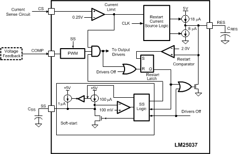 Figure 12. Current Limit Restart Circuit
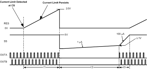 Figure 13. Current Limit Restart Timing
7.3.7 Soft-Start
The soft-start circuit allows the regulator to gradually reach a steady-state operating point, thereby reducing start-up stresses and current surges. When bias is supplied to the LM25037, the SS pin capacitor is discharged by an internal MOSFET. When the UVLO, VCC and REF pins reach their operating thresholds, the SS capacitor is released and charged with a 100-µA current source. The PWM comparator control voltage at the COMP pin is clamped to the SS pin voltage by an internal amplifier. When the PWM comparator input reaches 1 V, output pulses commence with slowly increasing duty cycle. The voltage at the SS pin eventually increases to 5 V, while the voltage at the PWM comparator increases to the value required for regulation as determined by the voltage feedback loop.
One method to disable the regulator is to ground the SS pin. This forces the internal PWM control signal to ground, reducing the output duty cycle quickly to zero. Releasing the SS pin initiates a soft-start sequence and normal operation resumes. A second shutdown method is discussed in UVLO Divider Selection.
7.3.8 PWM Comparator
The pulse width modulation (PWM) comparator compares the voltage ramp signal at the RAMP pin to the loop error signal. The loop error signal is derived from the internal error amplifier (COMP pin). The resulting control voltage passes through a 1-V level shift before being applied to the PWM comparator. This comparator is optimized for speed to achieve minimum controllable duty cycles. The common mode input voltage range of the PWM comparator is from 0 V to 4.3 V.
7.3.9 RAMP Pin
The voltage at the RAMP pin provides the modulation ramp for the PWM comparator. The PWM comparator compares the modulation ramp signal at the RAMP pin to the loop error signal to control the output duty cycle. The modulation ramp can be implemented either as a ramp proportional to input voltage, known as feed-forward voltage mode control, or as a ramp proportional to the primary current, known as current mode control. The RAMP pin is reset by an internal FET with an RDS(ON) of 5 Ω (typical) at the end of every cycle. The ability to configure the RAMP pin for either voltage mode or current mode allows the controller to be implemented for the optimum control method for the selected power stage topology. Configuring RAMP pin is explained below and the differences between voltage mode control and current mode control in various double-ended topologies is explained in Application and Implementation.
7.4 Device Functional Modes
7.4.1 Feed-Forward Voltage Mode
An external resistor (RFF) and capacitor (CFF) connected to VIN, AGND, and the RAMP pins is required to create the PWM ramp signal as shown in Figure 14. It can be seen that the slope of the signal at RAMP will vary in proportion to the input line voltage. This varying slope provides line feed-forward information necessary to improve line transient response with voltage mode control. The RAMP signal is compared to the error signal by the pulse width modulator comparator to control the duty cycle of the outputs. With a constant error signal, the on-time (tON) varies inversely with the input voltage (VIN) to stabilize the Volt • Second product of the transformer primary. At the end of clock period, an internal FET will be enabled to reset the CFF capacitor. The formulae for RFF and CFF and component selection criteria are explained in the Application and Implementation section. The amplitude of the signal driving RAMP pin must not exceed the common mode input voltage range of the PWM comparator (3.3 V) while in normal operation.
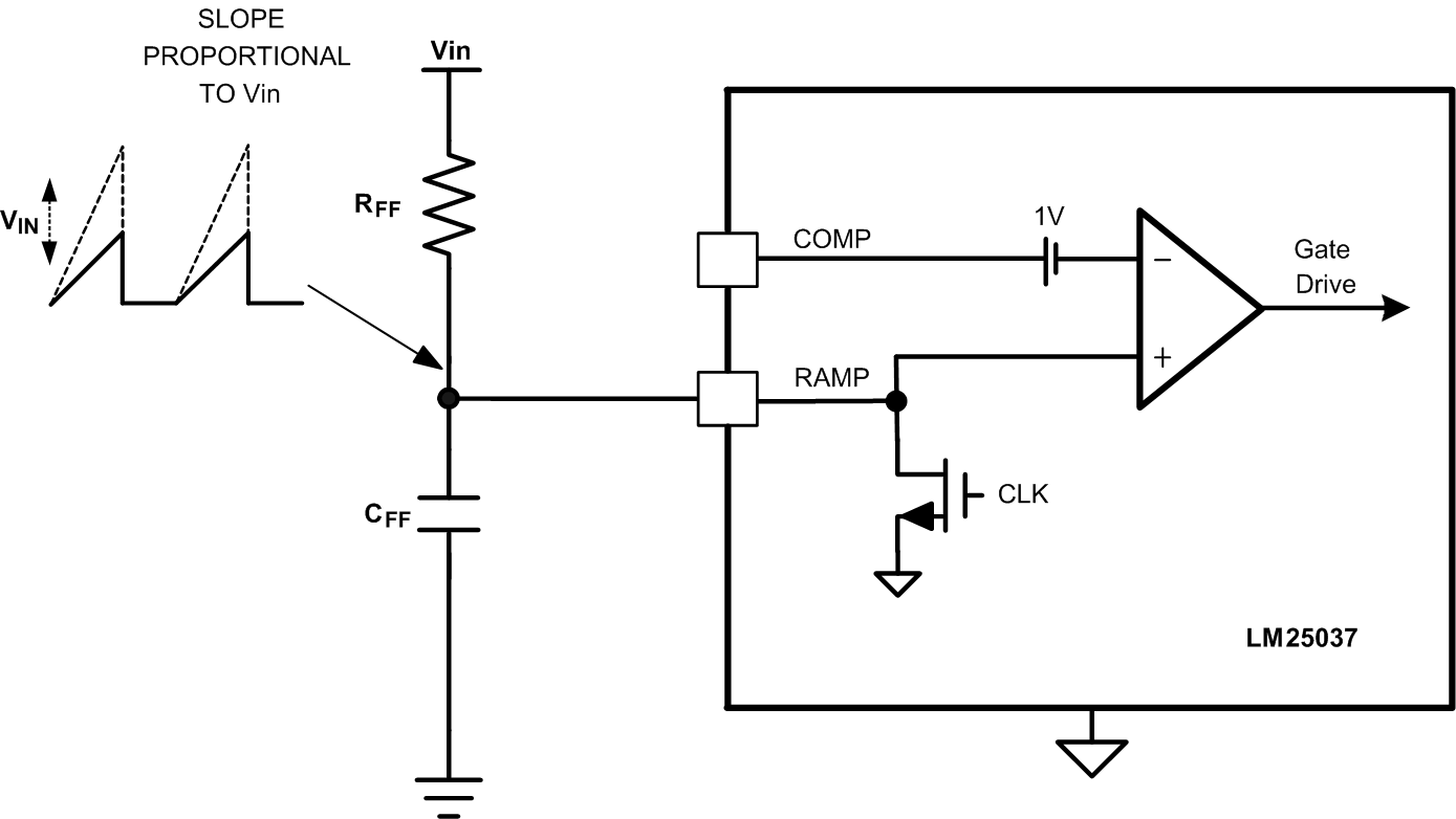 Figure 14. Feed-Forward Voltage Mode Configuration
7.4.2 Current Mode
The LM25037 can be configured for current mode control by injecting a signal representative of primary current into the RAMP pin. One way to achieve this is shown in Figure 15. Filter components Rfilter and Cfilter are used to filter leading edge noise spikes. The signal at the CS pin is thus a ramp on a pedestal. The pedestal corresponds to the continuous conduction current in the transformer at the beginning of an OUTA or OUTB conduction cycle. The R-C circuit (RSlope and CSlope), shown in Figure 15, tied to VREF adds an additional ramp to the current sense signal. This additional ramp signal, known as slope compensation, is required to avoid instabilities at duty cycles above 50% (25% per phase). The compensated RAMP signal consists of two parts, the primary current signal and the slope compensation. The compensated RAMP signal is compared to the error signal by the PWM comparator to control the duty cycle of the outputs. The RAMP capacitor and CS capacitor are reset through internal discharge FETs. The RDS(ON) of RAMP discharge FET is 5 Ω (typical); this ensures fast discharge of the RAMP reset capacitor. Any DC voltage source can be used in place of VREF to generate the slope compensation ramp.
The timing diagram shown in Figure 16 depicts the current mode waveforms and relative timing. When OUTA or OUTB is enabled, the signal at the RAMP pin consists of the CS pin signal (current ramp on a pedestal) plus the slope compensation ramp (dotted lines). When OUTA or OUTB is turned off, the primary current component is absent but the voltage at the RAMP pin continues to rise due to slope compensation component until the end of the clock period, after which it is reset by the RAMP discharge FET. A component selection example is explained in detail in Application and Implementation.
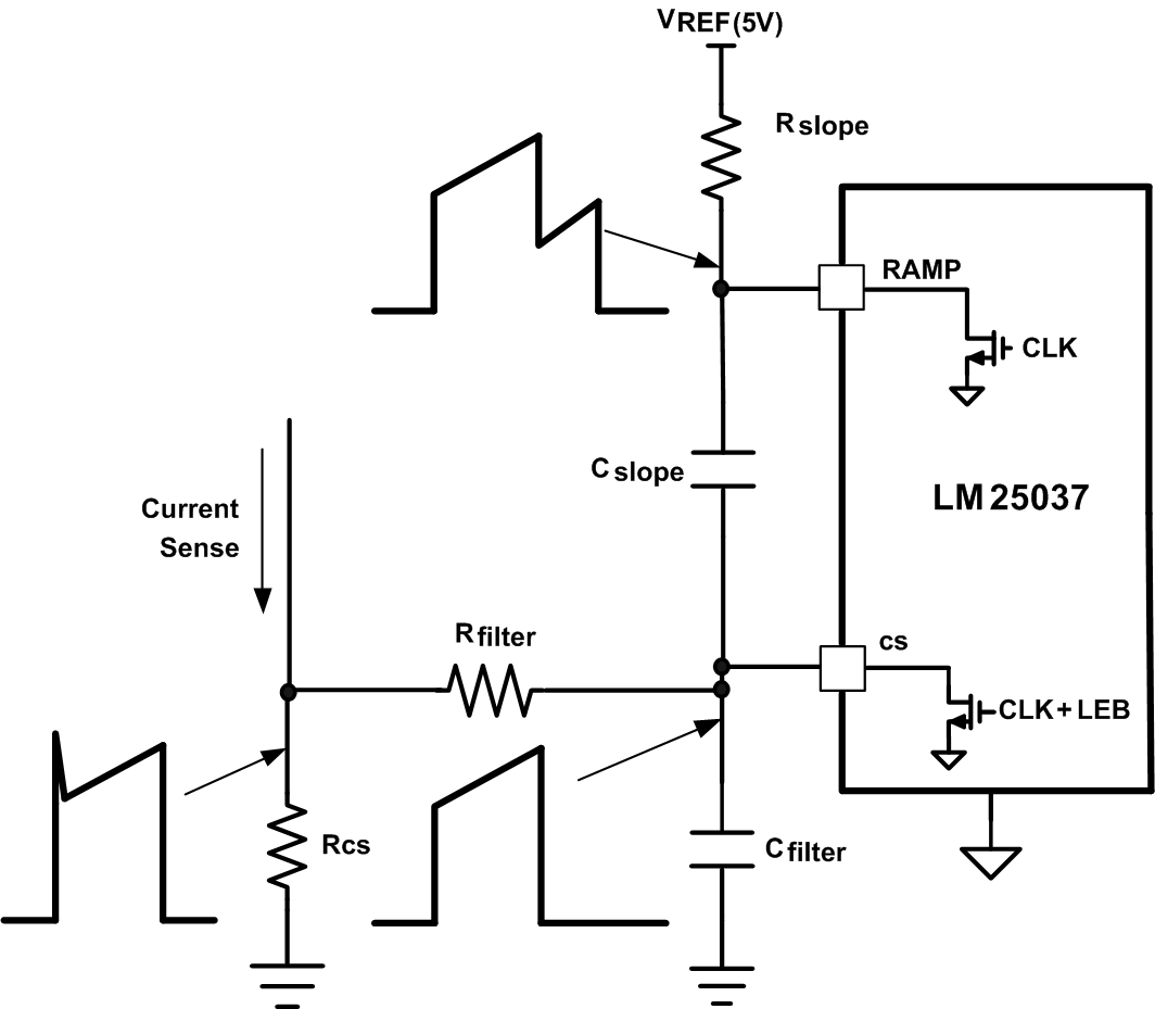 Figure 15. Current Mode Configuration With Slope Compensation
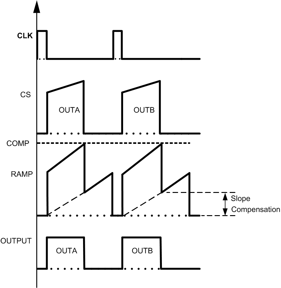 Figure 16. Timing Diagram for Current Mode Configuration
7.4.3 Oscillator
The LM25037 oscillator frequency and the maximum duty cycle are set by two external resistors connected between the RT1 and RT2 pins to AGND. The minimum dead-time between OUTA and OUTB pulses is proportional to the RT2 resistor value and the overall oscillator frequency is inversely proportional to RT1 and RT2 resistor values. Each output switches at half the oscillator frequency. Initially, RT2 should be selected for the desired dead-time or for the desired maximum duty cycle (Dmax), as given by Equation 1.

TI recommends setting the dead-time range from 50 ns to 250 ns. Beyond 250 ns, RT2 becomes excessively large, and is prone to noise pickup. Fixed internal delays limit the dead-time to greater than 50 ns. After the dead-time has been programmed by RT2, the overall oscillator frequency can be set by selecting resistor RT1 from Equation 2:

For example, if the desired oscillator frequency is 400 kHz (OUTA and OUTB each switching at 200 kHz) and desired dead-time is 100 ns, the maximum duty cycle for each output will be 96% and the values of RT1 and RT2 will be 15 kΩ and 20 kΩ respectively.
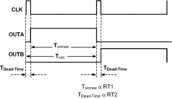 Figure 17. Timing Diagram of OUTA, OUTB and Dead-Time Set By RT2
As shown in Figure 17, the internal clock pulse width is the same as the dead-time set by RT2. This dead-time pulse is used to limit the maximum duty cycle for each of the outputs. Also, the discharge FET connected to the RAMP pin is enabled during the dead-time every clock period. The voltages at both the RT1 and RT2 pins are internally regulated to a nominal 2 V. Both the resistors RT1 and RT2 should be located as close as possible to the IC, and connected directly to the pins. The tolerance of the external resistors and the frequency tolerance indicated in Electrical Characteristics must be considered when determining the worst case frequency range.
7.4.4 Sync Capability
The LM25037 can be synchronized to an external clock by applying a narrow AC pulse to the RT1 pin. The external clock must be at least 10% higher than the free-running oscillator frequency set by the RT1 and RT2 resistors. If the external clock frequency is less than the programmed frequency, the LM25037 will ignore the synchronizing pulses. The synchronization pulse width at the RT1 pin must be a minimum of 15-ns wide. The synchronization signal should be coupled into the RT1 pin through a 100-pF capacitor or another value small enough to ensure the sync pulse width at RT1 is less than 60% of the clock period under all conditions. When the synchronizing pulse transitions from low-to-high (rising edge), the voltage at the RT1 pin must be driven to exceed 3 V from its nominal 2-V DC level. During the synchronization clock signal’s low time, the voltage at the RT1 pin will be clamped at 2 V by an internal regulator. The RT1 and RT2 resistors are always required, whether the oscillator is free running or externally synchronized.
7.4.5 Gate Driver Outputs (OUTA and OUTB)
The LM25037 provides two alternating gate driver outputs, OUTA and OUTB. The internal gate drivers can each source and sink 1.2-A peak each. The maximum duty cycle is inherently limited to less than 50% and is based on the value of RT2 resistor. As an example, if the COMP pin is in a high state, RT1 = 15 K and RT2 = 20 K then the outputs will operate at maximum duty cycle of 96%.
7.4.6 Thermal Protection
Internal Thermal Shutdown circuitry is provided to protect the integrated circuit in the event the maximum rated junction temperature is exceeded. When activated, typically at 165°C, the controller is forced into a low power standby state with the output drivers (OUTA and OUTB) and the bias regulators (VCC and REF) disabled. This helps to prevent catastrophic failures from accidental device overheating. During thermal shutdown, the soft-start capacitor is fully discharged and the controller follows a normal start-up sequence after the junction temperature falls to the operating level (140°C).