SNVS572E July 2008 – January 2016 LM25037 , LM25037-Q1
PRODUCTION DATA.
- 1 Features
- 2 Applications
- 3 Description
- 4 Revision History
- 5 Pin Configuration and Functions
- 6 Specifications
- 7 Detailed Description
- 8 Application and Implementation
- 9 Power Supply Recommendations
- 10Layout
- 11Device and Documentation Support
- 12Mechanical, Packaging, and Orderable Information
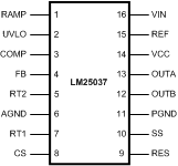
5 Pin Configuration and Functions
PW Package
16-Pin TSSOP
Top View

Pin Functions
| PIN | I/O | DESCRIPTION | APPLICATION INFORMATION | |
|---|---|---|---|---|
| NO. | NAME | |||
| 1 | RAMP | I | Pulse width modulator ramp | Modulation ramp for the PWM comparator. This ramp can be a representative of the primary current (current mode) or proportional to input voltage (feed-forward voltage mode). This pin is reset to ground at the conclusion of every cycle by an internal FET. |
| 2 | UVLO | I | Line undervoltage lockout | An external voltage divider from the power source sets the shutdown and standby comparator threshold levels. When UVLO exceeds the 0.45V shutdown threshold, the VCC and REF regulators are enabled. When UVLO exceeds the 1.25V standby threshold, the SS pin is released and the device enters the active mode. |
| 3 | COMP | I/O | Input to the pulse width modulator | Output of the error amplifier and input to the PWM comparator. |
| 4 | FB | I | Feedback | Connected to inverting input of the error amplifier. An internal 1.25-V reference is connected to the noninverting input of the error amplifier. In isolated applications using an external error amplifier, this pin should be connected to the AGND pin. |
| 5 | RT2 | I | Oscillator dead-time control | The resistance connected between RT2 and AGND sets the forced dead-time between switching periods of the alternating outputs. |
| 6 | AGND | — | Analog ground | Connect directly to Power Ground. |
| 7 | RT1 | I | Oscillator maximum on-time control | The resistance connected between RT1 and AGND sets the oscillator maximum on-time. The sum of this maximum on-time and the forced dead-time (set by RT2) sets the oscillator period. |
| 8 | CS | I | Current sense input | If CS exceeds 250 mV the output pulse will be terminated, entering cycle-by-cycle current limit. An internal switch holds CS low for 65 nS after either output switches high to blank leading edge transients. |
| 9 | RES | I/O | Restart timer | If cycle-by-cycle current limit is reached during any cycle, a 18-µA current is sourced to the external RES pin capacitor. If the RES capacitor voltage reaches 2 V, the soft-start capacitor will be fully discharged and then released with a pullup current of 1 uA. After the first output pulse (when SS = 1V), the SS pin charging current will increase to the normal level of 100 µA. |
| 10 | SS | I | Soft-start | An external capacitor and an internal 100uA current source set the soft-start ramp. The SS current source is reduced to 1 µA following a restart event (RES pin high). |
| 11 | PGND | — | Power ground | Connect directly to Analog Ground |
| 12 | OUTB | O | Output driver | Alternating gate drive output of the pulse width modulator. Capable of 1.2-A peak source and sink current. |
| 13 | OUTA | O | Output driver | Alternating gate drive output of the pulse width modulator. Capable of 1.2-A peak source and sink current. |
| 14 | VCC | I/O | Output of the high voltage start-up regulator. The VCC voltage is regulated to 7.7 V. | If an auxiliary winding raises the voltage on this pin above the regulation set point, the internal start-up regulator will shutdown thus reducing the IC power dissipation. Locally decouple VCC with a 0.47 µF or greater capacitor. |
| 15 | REF | O | Output of a 5-V reference | Locally decouple with a 0.1 µF or greater capacitor. Maximum output current is 10 mA (typical). |
| 16 | VIN | I | Input voltage source | Input to the VCC Start-up regulator. Operating input range is 5.5 V to 75 V. For power sources outside of this range, the LM25037 can be biased directly at VCC by an external regulator. |