ZHCSFK2C July 2012 – September 2016 LM25101
PRODUCTION DATA.
- 1 特性
- 2 应用
- 3 说明
- 4 修订历史记录
- 5 Device Options
- 6 Pin Configuration and Functions
- 7 Specifications
- 8 Detailed Description
- 9 Application and Implementation
- 10Power Supply Recommendations
- 11Layout
- 12器件和文档支持
- 13机械、封装和可订购信息
封装选项
机械数据 (封装 | 引脚)
散热焊盘机械数据 (封装 | 引脚)
- DGN|8
订购信息
9 Application and Implementation
NOTE
Information in the following applications sections is not part of the TI component specification, and TI does not warrant its accuracy or completeness. TI’s customers are responsible for determining suitability of components for their purposes. Customers should validate and test their design implementation to confirm system functionality.
9.1 Application Information
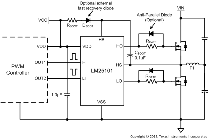
The LM25101 is a high voltage gate driver designed to drive both the high-side and low-side N-Channel MOSFETs in a half or full bridge configuration or in a synchronous buck circuit. The floating high side driver is capable of operating with supply voltages up to 100 V. This allows for N-Channel MOSFETs control in half-bridge, full-bridge, push-pull, two switch forward, and active clamp topologies. The outputs are independently controlled. Each channel is controlled by its respective input pins (HI and LI), allowing full and independent flexibility to control the state (ON and OFF) of the output.
9.2 Typical Application
 Figure 21. Application Diagram
9.2.1 Design Requirements
For this design example, use the parameters listed in Table 5 as the input parameters.
Table 5. Design Parameters
| PARAMETER | EXAMPLE VALUE |
|---|---|
| Gate driver | LM25101 (C version) |
| MOSFET | CSD19534KCS |
| VDD | 10 V |
| QG | 17 nC |
| fSW | 500 kHz |
9.2.2 Detailed Design Procedure
9.2.2.1 Selecting External Gate Driver Resistor
External gate driver resistor (RGATE) is sized to reduce ringing caused by parasitic inductances and capacitances and also to limit the current coming out of the gate driver.
Peak HO pullup current is calculated using Equation 1.

where
- IOHHis the peak pullup current
- VDHis the bootstrap diode forward voltage drop
- RHOHis the gate driver internal HO pullup resistance (1)
- RGateis the external gate drive resistance
- R(GFET_Int) is the MOSFET internal gate resistance, provided by the transistor data sheet
Similarly, Peak HO pulldown current is calculated using Equation 2.

where
- RHOL is the HO pulldown resistance
Peak LO pullup current is calculated using Equation 3.

where
- RLOH is the LO pullup resistance
Peak LO pulldown current is calculated using Equation 4.

where
- RLOL is the LO pulldown resistance
If the application requires fast turnoff, an anti-paralleled diode on RGate may be used to bypass the external gate drive resistor and speed up the turnoff transition.
9.2.3 Application Curves
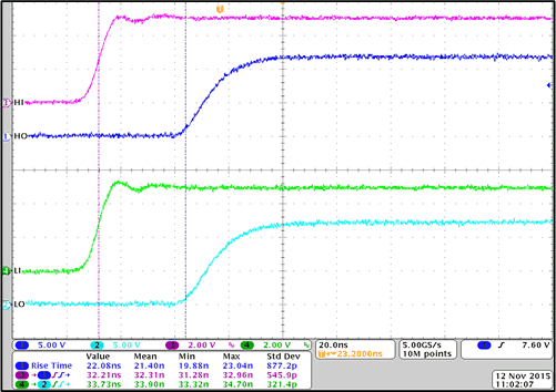
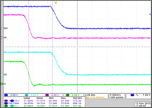
Figure 22 and Figure 23 show the rising and falling time and turnon and turnoff propagation delay testing waveform at room temperature. Each channel (HI, LI, HO, LO) is labeled and displayed on the left hand of the waveform.
The HI and LI pins are shorted together for these test waveforms. Therefore, the propagation delay matching between the channels can be measured and inspected.

| CL = 1 nF | VDD = 12 V | fSW = 500 kHz |

| CL = 1 nF | VDD = 12 V | fSW = 500 kHz |