ZHCSFK2C July 2012 – September 2016 LM25101
PRODUCTION DATA.
- 1 特性
- 2 应用
- 3 说明
- 4 修订历史记录
- 5 Device Options
- 6 Pin Configuration and Functions
- 7 Specifications
- 8 Detailed Description
- 9 Application and Implementation
- 10Power Supply Recommendations
- 11Layout
- 12器件和文档支持
- 13机械、封装和可订购信息
封装选项
机械数据 (封装 | 引脚)
散热焊盘机械数据 (封装 | 引脚)
- DGN|8
订购信息
11 Layout
11.1 Layout Guidelines
The optimum performance of high and low-side gate drivers cannot be achieved without following certain guidelines during circuit-board layout.
- Low ESR and ESL capacitors must be connected close to the IC, between the VDD and VSS pins and between the HB and HS pins to support the high peak currents being drawn from VDD during start-up of the external MOSFET.
- To prevent large voltage transients at the drain of the top MOSFET, a low ESR electrolytic capacitor must be connected between the MOSFET drain and ground (VSS).
- To avoid large negative transients on the switch node (HS pin), the parasitic inductances must be minimized in the source of the top MOSFET and in the drain of the bottom MOSFET (synchronous rectifier).
- Grounding Considerations:
- The first priority in designing grounding connections is to confine to a minimal physical area the high peak currents that charge and discharge the MOSFET gate. This decreases the loop inductance and minimizes noise issues on the gate terminal of the MOSFET. The MOSFETs should be placed as close as possible to the gate driver.
- The second high current path includes the bootstrap capacitor, the bootstrap diode, the local ground referenced bypass capacitor, and low-side MOSFET body diode. The bootstrap capacitor is recharged on a cycle-by-cycle basis through the bootstrap diode from the ground referenced VDD bypass capacitor. The recharging occurs in a short time interval and involves high peak current. Minimizing this loop length and area on the circuit board is important to ensure reliable operation.
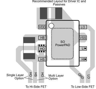
Figure 26 shows a recommended layout pattern for the driver. If possible a single layer placement is preferred.
11.2 Layout Example
 Figure 26. Recommended Layout Pattern