ZHCSFK2C July 2012 – September 2016 LM25101
PRODUCTION DATA.
- 1 特性
- 2 应用
- 3 说明
- 4 修订历史记录
- 5 Device Options
- 6 Pin Configuration and Functions
- 7 Specifications
- 8 Detailed Description
- 9 Application and Implementation
- 10Power Supply Recommendations
- 11Layout
- 12器件和文档支持
- 13机械、封装和可订购信息
封装选项
机械数据 (封装 | 引脚)
散热焊盘机械数据 (封装 | 引脚)
- DGN|8
订购信息
7 Specifications
7.1 Absolute Maximum Ratings
over operating free-air temperature range (unless otherwise noted)(1)| MIN | MAX | UNIT | |
|---|---|---|---|
| VDD to VSS | −0.3 | 18 | V |
| HB to HS | −0.3 | 18 | V |
| LI or HI Input | −0.3 | VDD + 0.3 | V |
| LO Output | −0.3 | VDD + 0.3 | V |
| HO Output | VHS - 0.3 | VHB + 0.3 | V |
| HS to VSS(2) | –5 | 100 | V |
| HB to VSS | 100 | V | |
| Junction temperature, TJ | 150 | °C | |
| Storage temperature, Tstg | –55 | 150 | °C |
(1) Stresses beyond those listed under Absolute Maximum Ratings may cause permanent damage to the device. These are stress ratings only, which do not imply functional operation of the device at these or any other conditions beyond those indicated under Recommended Operating Conditions. Exposure to absolute-maximum-rated conditions for extended periods may affect device reliability. For performance limits and associated test conditions, see the Electrical Characteristics tables.
7.2 ESD Ratings
| VALUE | UNIT | ||||
|---|---|---|---|---|---|
| V(ESD) | Electrostatic discharge | Human-body model (HBM), per ANSI/ESDA/JEDEC JS-001(1) | All pins except 2, 3, and 4 | ±2000 | V |
| Pins 2, 3, and 4 | ±1000 | ||||
| Charged-device model (CDM), per JEDEC specification JESD22-C101(2) | ±250 | ||||
| Machine model (MM) | ±100 | ||||
(1) The Human Body Model (HBM) is a 100-pF capacitor discharged through a 1.5-kΩ resistor into each pin.
(2) JEDEC document JEP157 states that 250-V CDM allows safe manufacturing with a standard ESD control process.
7.3 Recommended Operating Conditions
over operating free-air temperature range (unless otherwise noted)| MIN | MAX | UNIT | |||
|---|---|---|---|---|---|
| VDD | Supply voltage | VDD | 9 | 14 | V |
| VHS | Voltage | HS | –1 | 100 – VDD | V |
| VHB | Voltage | HB | VHS + 8 | VHS + 14 | V |
| HS slew rate | 50 | V/ns | |||
| TJ | Junction temperature | –40 | 125 | °C | |
7.4 Thermal Information
| THERMAL METRIC(1) | LM25101A, LM25101B | LM25101C | UNIT | ||||||
|---|---|---|---|---|---|---|---|---|---|
| D (SOIC) | DDA (SO PowerPAD) | NGT (WSON) | DPR (WSON) | D (SOIC) | DPR (WSON) | DGN (MSOP PowerPAD) | |||
| 8 PINS | 8 PINS | 8 PINS | 10 PINS | 8 PINS | 10 PINS | 8 PINS | |||
| RθJA | Junction-to-ambient thermal resistance | 108.2 | 46.1 | 38.2 | 37.8 | 111.5 | 39.8 | 54.1 | °C/W |
| RθJC(top) | Junction-to-case (top) thermal resistance | 50.6 | 53.5 | 36.3 | 35.8 | 54.2 | 39.1 | 55.9 | °C/W |
| RθJB | Junction-to-board thermal resistance | 49.1 | 13.8 | 15.2 | 15.0 | 52.3 | 17.1 | 15.1 | °C/W |
| ψJT | Junction-to-top characterization parameter | 7.6 | 4.2 | 0.3 | 0.3 | 9.0 | 0.4 | 2.4 | °C/W |
| ψJB | Junction-to-board characterization parameter | 48.5 | 13.9 | 15.4 | 15.3 | 51.7 | 17.3 | 15.1 | °C/W |
| RθJC(bot) | Junction-to-case (bottom) thermal resistance | — | 3.9 | 4.5 | 4.4 | — | 6.1 | 4.6 | °C/W |
(1) For more information about traditional and new thermal metrics, see the Semiconductor and IC Package Thermal Metrics application report.
7.5 Electrical Characteristics
Typical values apply for TJ = 25°C only. Minimum and maximum limits apply for TJ= –40°C to 125°C.(1) Unless otherwise specified, VDD = VHB = 12 V, VSS = VHS = 0 V, No Load on LO or HO.| PARAMETER | TEST CONDITIONS | MIN | TYP | MAX | UNIT | ||
|---|---|---|---|---|---|---|---|
| SUPPLY CURRENTS | |||||||
| IDD | VDD quiescent current | VLI = VHI = 0 V | 0.25 | 0.4 | mA | ||
| IDDO | VDD operating current | f = 500 kHz | 2.0 | 3 | mA | ||
| IHB | Total HB quiescent current | VLI = VHI = 0 V | 0.06 | 0.2 | mA | ||
| IHBO | Total HB operating current | f = 500 kHz | 1.6 | 3 | mA | ||
| IHBS | HB to VSS current (quiescent) | VHS = VHB = 100 V | 0.1 | 10 | µA | ||
| IHBSO | HB to VSS current (operating) | f = 500 kHz | 0.4 | mA | |||
| INPUT PINS | |||||||
| VIL | Input voltage threshold | Rising Edge | 1.3 | 1.8 | 2.3 | V | |
| VIHYS | Input voltage hysteresis | 50 | mV | ||||
| RI | Input pulldown resistance | 100 | 200 | 400 | kΩ | ||
| UNDER VOLTAGE PROTECTION | |||||||
| VDDR | VDD rising threshold | 6.0 | 6.9 | 7.4 | V | ||
| VDDH | VDD threshold hysteresis | 0.5 | V | ||||
| VHBR | HB rising threshold | 5.7 | 6.6 | 7.1 | V | ||
| VHBH | HB threshold hysteresis | 0.4 | V | ||||
| BOOT STRAP DIODE | |||||||
| VDL | Low-current forward voltage | IVDD-HB = 100 µA | 0.52 | 0.85 | V | ||
| VDH | High-current forward voltage | IVDD-HB = 100 mA | 0.8 | 1 | V | ||
| RD | Dynamic resistance | IVDD-HB = 100 mA | 1.0 | 1.65 | Ω | ||
| LO AND HO GATE DRIVER | |||||||
| VOL | Low-level output voltage | IHO = ILO = 100 mA | A version | 0.12 | 0.25 | V | |
| B version | 0.16 | 0.4 | |||||
| C version | 0.28 | 0.65 | |||||
| VOH | High-level output voltage | IHO = ILO = 100 mA VOH = VDD – VLO or VOH = VHB – VHO |
A version | 0.24 | 0.45 | V | |
| B version | 0.28 | 0.60 | |||||
| C version | 0.60 | 1.10 | |||||
| IOHL | Peak pullup current | HO, VLO = 0 V | A version | 3 | A | ||
| B version | 2 | ||||||
| C version | 1 | ||||||
| IOLL | Peak pulldown current | HO, VLO = 12 V | A version | 3 | A | ||
| B version | 2 | ||||||
| C version | 1 | ||||||
7.6 Switching Characteristics
Typical values apply for TJ = 25°C only. Minimum and maximum limits apply for TJ= –40°C to 125°C.(1) Unless otherwise specified, VDD = VHB = 12 V, VSS = VHS = 0 V, No Load on LO or HO.| PARAMETER | TEST CONDITIONS | MIN | TYP | MAX | UNIT | ||
|---|---|---|---|---|---|---|---|
| tLPHL | LO turnoff propagation delay | LI falling to LO falling | 22 | 56 | ns | ||
| tLPLH | LO turnon propagation delay | LI rising to LO rising | 26 | 56 | ns | ||
| tHPHL | HO turnoff propagation delay | HI falling to HO falling | 22 | 56 | ns | ||
| tHPLH | LO turnon propagation delay | HI rising to HO rising | 26 | 56 | ns | ||
| tMON | Delay matching | LO ON and HO OFF | 4 | 10 | ns | ||
| tMOFF | Delay matching | LO OFF and HO ON | 4 | 10 | ns | ||
| tRC, tFC | Either output rise and fall time | CL = 1000 pF | 8 | ns | |||
| tR | Output rise time (3 V to 9 V) | CL = 0.1 µF | A version | 430 | ns | ||
| B version | 570 | ||||||
| C version | 990 | ||||||
| tF | Output fall time (3 V to 9 V) | CL = 0.1 µF | A version | 260 | ns | ||
| B version | 430 | ||||||
| C version | 715 | ||||||
| tPW | Minimum input pulse duration that changes the output | 50 | ns | ||||
| tBS | Bootstrap diode reverse recovery time | IF = 100 mA, IR = 100 mA | 37 | ns | |||
(1) Minimum and maximum limits are 100% production tested at 25°C. Limits over the operating temperature range are specified through correlation using Statistical Quality Control (SQC) methods. Limits are used to calculate Average Outgoing Quality Level (AOQL).
(2) In the application the HS node is clamped by the body diode of the external lower N-MOSFET, therefore the HS node will generally not exceed –1 V. However, in some applications, board resistance and inductance may result in the HS node exceeding this stated voltage transiently. If negative transients occur, the HS voltage must never be more negative than VDD – 15 V. For example, if VDD = 10 V, the negative transients at HS must not exceed –5 V.
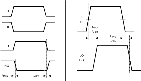 Figure 1. Timing Diagram
7.7 Typical Characteristics
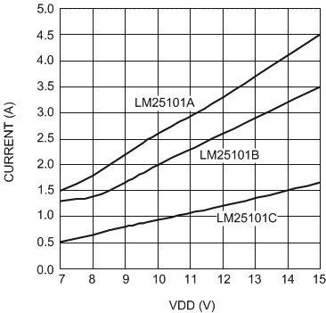 Figure 2. Peak Sourcing Current vs Supply Voltage
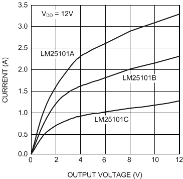 Figure 4. Sink Current vs Output Voltage
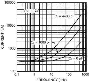 Figure 6. IDD vs Frequency
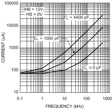 Figure 8. IHB vs Frequency
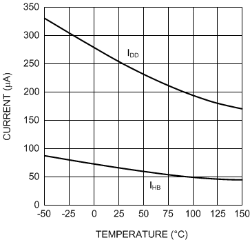 Figure 10. Quiescent Current vs Temperature
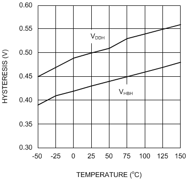 Figure 12. Undervoltage Threshold Hysteresis
vs Temperature
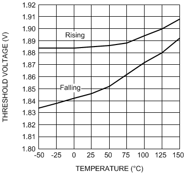 Figure 14. Input Threshold vs Temperature
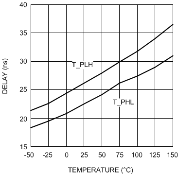 Figure 16. Propagation Delay vs Temperature
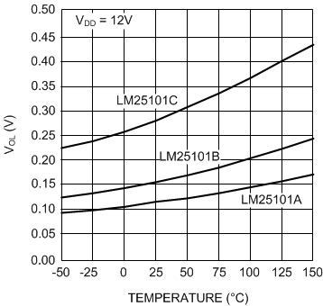 Figure 18. LO and HO Gate Drive:
Low Level Output Voltage vs Temperature
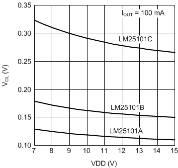 Figure 20. LO and HO Gate Drive:
Output Low Voltage vs Supply Voltage
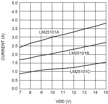 Figure 3. Peak Sinking Current vs Supply Voltage
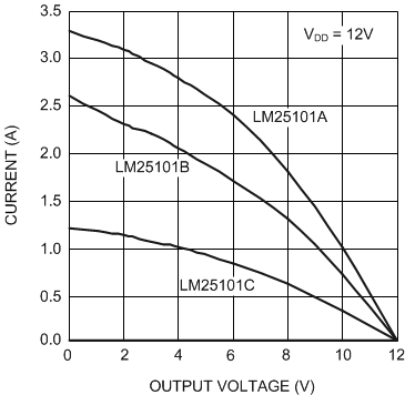 Figure 5. Source Current vs Output Voltage
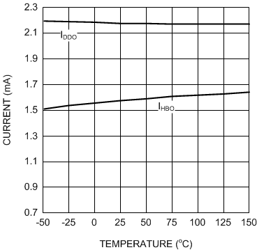 Figure 7. Operating Current vs Temperature
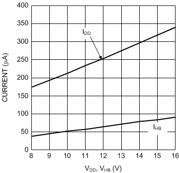 Figure 9. Quiescent Current vs Supply Voltage
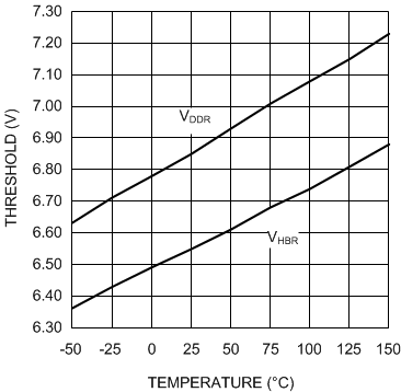 Figure 11. Undervoltage Rising Thresholds
vs Temperature
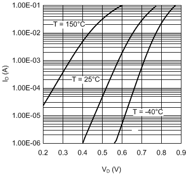 Figure 13. Bootstrap Diode Forward Voltage
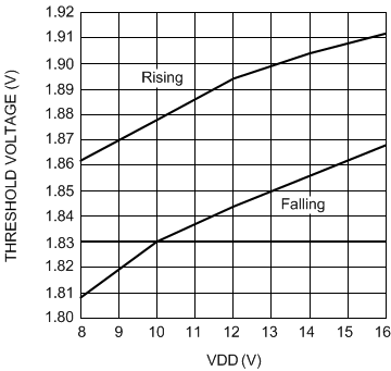 Figure 15. Input Threshold vs Supply Voltage
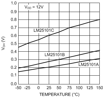 Figure 17. LO and HO Gate Drive:
High Level Output Voltage vs Temperature
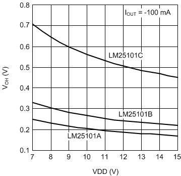 Figure 19. LO and HO Gate Drive:
Output High Voltage vs Supply Voltage