ZHCSGG8F July   2011  – March 2018 LM25118

PRODUCTION DATA.  

  1. 特性
  2. 应用
  3. 说明
    1.     Device Images
      1.      简化原理图
      2.      效率与输入电压和输出电流(输出电压 = 12V)
  4. 修订历史记录
  5. Pin Configuration and Functions
    1.     Pin Functions
  6. Specifications
    1. 6.1 Absolute Maximum Ratings
    2. 6.2 ESD Ratings
    3. 6.3 Recommended Operating Conditions
    4. 6.4 Thermal Information
    5. 6.5 Electrical Characteristics
    6. 6.6 Typical Characteristics
  7. Detailed Description
    1. 7.1 Overview
    2. 7.2 Functional Block Diagram
    3. 7.3 Feature Description
      1. 7.3.1 UVLO
      2. 7.3.2 Oscillator and Sync Capability
      3. 7.3.3 Error Amplifier and PWM Comparator
      4. 7.3.4 Ramp Generator
      5. 7.3.5 Current Limit
      6. 7.3.6 Maximum Duty Cycle
      7. 7.3.7 Soft Start
      8. 7.3.8 HO Output
      9. 7.3.9 Thermal Protection
    4. 7.4 Device Functional Modes
      1. 7.4.1 Buck Mode Operation: VIN > VOUT
      2. 7.4.2 Buck-Boost Mode Operation: VIN ≊ VOUT
      3. 7.4.3 High Voltage Start-Up Regulator
      4. 7.4.4 Enable
  8. Application and Implementation
    1. 8.1 Application Information
    2. 8.2 Typical Application
      1. 8.2.1 Design Requirements
      2. 8.2.2 Detailed Design Procedure
        1. 8.2.2.1  Custom Design With WEBENCH® Tools
        2. 8.2.2.2  R7 = RT
        3. 8.2.2.3  Inductor Selection – L1
        4. 8.2.2.4  R13 = RSENSE
        5. 8.2.2.5  C15 = CRAMP
        6. 8.2.2.6  Inductor Current Limit Calculation
        7. 8.2.2.7  C9 - C12 = Output Capacitors
        8. 8.2.2.8  D1
        9. 8.2.2.9  D4
        10. 8.2.2.10 C1 – C5 = Input Capacitors
        11. 8.2.2.11 C20
        12. 8.2.2.12 C8
        13. 8.2.2.13 C16 = CSS
        14. 8.2.2.14 R8, R9
        15. 8.2.2.15 R1, R3, C21
        16. 8.2.2.16 R2
        17. 8.2.2.17 Snubber
        18. 8.2.2.18 Error Amplifier Configuration
          1. 8.2.2.18.1 R4, C18, C17
      3. 8.2.3 Application Curves
  9. Power Supply Recommendations
    1. 9.1 Bias Power Dissipation Reduction
    2. 9.2 Thermal Considerations
  10. 10Layout
    1. 10.1 Layout Guidelines
    2. 10.2 Layout Example
  11. 11器件和文档支持
    1. 11.1 器件支持
      1. 11.1.1 开发支持
        1. 11.1.1.1 使用 WEBENCH® 工具创建定制设计
    2. 11.2 接收文档更新通知
    3. 11.3 社区资源
    4. 11.4 商标
    5. 11.5 静电放电警告
    6. 11.6 Glossary
  12. 12机械、封装和可订购信息

封装选项

机械数据 (封装 | 引脚)
散热焊盘机械数据 (封装 | 引脚)
订购信息

Application Curves

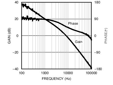
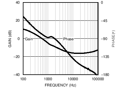
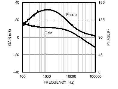
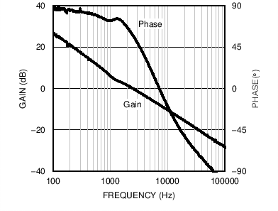
The plots shown in Figure 21 through Figure 26 show the gain and phase diagrams of the design example. The overall bandwidth is lower in a buck-boost application due the compensation challenges associated with the right-half-plane zero. For a pure buck application, the bandwidth could be much higher. The LM5116 data sheet is a good reference for compensation design of a pure buck mode regulator.
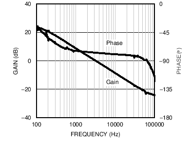
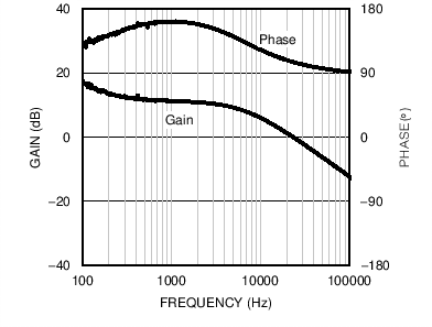
LM25118 21 Mod Buck.pngFigure 21. Modulator Gain and Phase - Buck Mode
LM25118 23 Error Amp Buck.pngFigure 23. Error Amplifier Gain and Phase - Buck Mode
LM25118 25 Overall Buck.pngFigure 25. Overall Loop Gain and Phase - Buck Mode
LM25118 22 Mod Buck Boost.pngFigure 22. Modulator Gain and Phase - Buck-Boost Mode
LM25118 24 Error Amp Buck Boost.pngFigure 24. Error Amplifier Gain and Phase - Buck-Boost Mode
LM25118 26 Overall Buck Boost.pngFigure 26. Overall Loop Gain and Phase - Buck-Boost Mode