ZHCS573I August 2010 – April 2018 LM25119
PRODUCTION DATA.
- 1 特性
- 2 应用
- 3 说明
- 4 修订历史记录
- 5 Pin Configuration and Functions
- 6 Specifications
-
7 Detailed Description
- 7.1 Overview
- 7.2 Functional Block Diagram
- 7.3
Feature Description
- 7.3.1 High Voltage Start-Up Regulator
- 7.3.2 UVLO
- 7.3.3 Enable 2
- 7.3.4 Oscillator and Sync Capability
- 7.3.5 Error Amplifiers and PWM Comparators
- 7.3.6 Ramp Generator
- 7.3.7 Current Limit
- 7.3.8 Hiccup Mode Current Limiting
- 7.3.9 Soft Start
- 7.3.10 HO and LO Output Drivers
- 7.3.11 Maximum Duty Cycle
- 7.3.12 Thermal Protection
- 7.4 Device Functional Modes
-
8 Application and Implementation
- 8.1 Application Information
- 8.2
Typical Applications
- 8.2.1
Dual-output Design Example
- 8.2.1.1 Design Requirements
- 8.2.1.2
Detailed Design Procedure
- 8.2.1.2.1 Timing Resistor
- 8.2.1.2.2 Output Inductor
- 8.2.1.2.3 Current Sense Resistor
- 8.2.1.2.4 Ramp Resistor and Ramp Capacitor
- 8.2.1.2.5 Output Capacitors
- 8.2.1.2.6 Input Capacitors
- 8.2.1.2.7 VCC Capacitor
- 8.2.1.2.8 Bootstrap Capacitor
- 8.2.1.2.9 Soft Start Capacitor
- 8.2.1.2.10 Restart Capacitor
- 8.2.1.2.11 Output Voltage Divider
- 8.2.1.2.12 UVLO Divider
- 8.2.1.2.13 MOSFET Selection
- 8.2.1.2.14 MOSFET Snubber
- 8.2.1.2.15 Error Amplifier Compensation
- 8.2.1.3 Application Curves
- 8.2.2 Two-Phase Design Example
- 8.2.1
Dual-output Design Example
- 9 Power Supply Recommendations
- 10Layout
- 11器件和文档支持
- 12机械、封装和可订购信息
8.1.2 Interleaved Two-Phase Operation
Interleaved operation offers many advantages in single-output, high-current applications. The output power path is split between two identical channels reducing the current in each channel by one-half. Ripple current reduction in the output capacitors is reduced significantly because each channel operates 180 degrees out of phase from the other. Ripple reduction is greatest at 50% duty cycle and decreases as the duty cycle varies away from 50%.
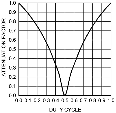
Refer to Figure 12 to estimate the ripple current reduction. Also, the effective ripple in the input and output capacitors occurs at twice the frequency of a single-channel design due to the combining of the two channels. All of these factors are advantageous in managing the higher currents and their effects in a high power design.
 Figure 12. Cancellation Factor vs Duty Cycle for Output Capacitor
To begin an interleaved design, use the previous equations in this datasheet to first calculate the required value of components using one-half the current in the output power path. The attenuation factor in Figure 12 is the ratio of the output capacitor ripple to the inductor ripple versus duty cycle. The inductor ripple used in this calculation is the ripple in either inductor in a two phase design, not the ripple calculated for a single phase design of the same output power. It can be observed that operation around 50% duty cycle results in almost complete ripple attenuation in the output capacitor. Figure 12 can be used to calculate the amount of ripple attenuation in the output capacitors.
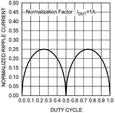
 Figure 13. Normalized Input Capacitor RMS Ripple Current vs Duty Cycle
Figure 13 illustrates the ripple current reduction in the input capacitors due to interleaving. As with the output capacitors, there is near perfect ripple reduction near 50% duty cycle. This plot can be used to calculate the ripple in the input capacitors at any duty cycle. In designs with large duty cycle swings, use the worst-case ripple reduction for the design.
To configure the LM25119 device for interleaved operation, connect COMP1 and COMP2 pins together at the IC. Connecting the FB2 pin to VCC2 pin disables the channel2 error amplifier with a high output impedance at COMP2. Connect the compensation network between FB1 and the common COMP pins. Connect the two power stages together at the output capacitors. Finally use the plots in Figure 12 and Figure 13 along with the duty cycle range to determine the amount of output and input capacitor ripple reduction. Frequently more capacitance than necessary is used in a design just to meet ESR requirements. Reducing the capacitance based solely on ripple reduction graphs alone may violate this requirement.