ZHCSEL4A December 2015 – December 2015 LM25122-Q1
PRODUCTION DATA.
- 1 特性
- 2 应用
- 3 说明
- 4 修订历史记录
- 5 Pin Configuration and Functions
- 6 Specifications
-
7 Detailed Description
- 7.1 Overview
- 7.2 Functional Block Diagram
- 7.3
Feature Description
- 7.3.1 Undervoltage Lockout (UVLO)
- 7.3.2 High Voltage VCC Regulator
- 7.3.3 Oscillator
- 7.3.4 Slope Compensation
- 7.3.5 Error Amplifier
- 7.3.6 PWM Comparator
- 7.3.7 Soft-Start
- 7.3.8 HO and LO Drivers
- 7.3.9 Bypass Operation (VOUT = VIN)
- 7.3.10 Cycle-by-Cycle Current Limit
- 7.3.11 Clock Synchronization
- 7.3.12 Maximum Duty Cycle
- 7.3.13 Thermal Protection
- 7.4 Device Functional Modes
-
8 Application and Implementation
- 8.1 Application Information
- 8.2
Typical Application
- 8.2.1 Design Requirements
- 8.2.2
Detailed Design Procedure
- 8.2.2.1 Timing Resistor RT
- 8.2.2.2 UVLO Divider RUV2, RUV1
- 8.2.2.3 Input Inductor LIN
- 8.2.2.4 Current Sense Resistor RS
- 8.2.2.5 Current Sense Filter RCSFP, RCSFN, CCS
- 8.2.2.6 Slope Compensation Resistor RSLOPE
- 8.2.2.7 Output Capacitor COUT
- 8.2.2.8 Input Capacitor CIN
- 8.2.2.9 VIN Filter RVIN, CVIN
- 8.2.2.10 Bootstrap Capacitor CBST and Boost Diode DBST
- 8.2.2.11 VCC Capacitor CVCC
- 8.2.2.12 Output Voltage Divider RFB1, RFB2
- 8.2.2.13 Soft-Start Capacitor CSS
- 8.2.2.14 Restart Capacitor CRES
- 8.2.2.15 Low-Side Power Switch QL
- 8.2.2.16 High-Side Power Switch QH and Additional Parallel Schottky Diode
- 8.2.2.17 Snubber Components
- 8.2.2.18 Loop Compensation Components CCOMP, RCOMP, CHF
- 8.2.3 Application Curves
- 9 Power Supply Recommendations
- 10Layout
- 11器件和文档支持
- 12机械、封装和可订购信息
8 Application and Implementation
NOTE
Information in the following applications sections is not part of the TI component specification, and TI does not warrant its accuracy or completeness. TI’s customers are responsible for determining suitability of components for their purposes. Customers should validate and test their design implementation to confirm system functionality.
8.1 Application Information
The LM25122 device is a step-up dc-dc converter. The device is typically used to convert a lower dc voltage to a higher dc voltage. Use the following design procedure to select component values for the LM25122 device. Alternately, use the WEBENCH® software to generate a complete design. The WEBENCH software uses an iterative design procedure and accesses a comprehensive database of components when generating a design. This section presents a simplified discussion of the design process.
8.1.1 Feedback Compensation
The open loop response of a boost regulator is defined as the product of modulator transfer function and feedback transfer function. When plotted on a dB scale, the open loop gain is shown as the sum of modulator gain and feedback gain. The modulator transfer function of a current mode boost regulator including a power stage transfer function with an embedded current loop can be simplified as one pole, one zero and one Right Half Plane (RHP) zero system.
Modulator transfer function is defined as follows:

where
-

-

-

-

-

- n is the number of the phase.
If the ESR of COUT (RESR) is small enough and the RHP zero frequency is far away from the target crossover frequency, the modulator transfer function can be further simplified to one pole system and the voltage loop can be closed with only two loop compensation components, RCOMP and CCOMP, leaving a single pole response at the crossover frequency. A single pole response at the crossover frequency yields a very stable loop with 90 degrees of phase margin.
The feedback transfer function includes the feedback resistor divider and loop compensation of the error amplifier. RCOMP, CCOMP and optional CHF configure the error amplifier gain and phase characteristics, create a pole at origin, a low frequency zero and a high frequency pole.
Feedback transfer function is defined as follows:

where
The pole at the origin minimizes the output steady state error. The low frequency zero should be placed to cancel the load pole of the modulator. The high frequency pole can be used to cancel the zero created by the output capacitor ESR or to decrease noise susceptibility of the error amplifier. By placing the low frequency zero an order of magnitude less than the crossover frequency, the maximum amount of phase boost can be achieved at the crossover frequency. The high frequency pole should be placed beyond the crossover frequency since the addition of CHF adds a pole in the feedback transfer function.
The crossover frequency (open loop bandwidth) is usually selected between one twentieth and one fifth of the fSW. In a simplified formula, the estimated crossover frequency can be defined as:

where
For higher crossover frequency, RCOMP can be increased, while proportionally decreasing CCOMP. Conversely, decreasing RCOMP while proportionally increasing CCOMP, results in lower bandwidth while keeping the same zero frequency in the feedback transfer function.
The modulator transfer function can be measured by a network analyzer and the feedback transfer function can be configured for the desired open loop transfer function. If the network analyzer is not available, step load transient tests can be performed to verify acceptable performance. The step load goal is minimum overshoot/undershoot with a damped response.
8.1.2 Sub-Harmonic Oscillation
Peak current mode regulator can exhibit unstable behavior when operating above 50% duty cycle. This behavior is known as sub-harmonic oscillation and is characterized by alternating wide and narrow pulses at the SW pin. Sub-harmonic oscillation can be prevented by adding an additional slope voltage ramp (slope compensation) on top of the sensed inductor current. By choosing K ≥ 0.82~1.0, the sub-harmonic oscillation will be eliminated even with wide varying input voltage.
In time-domain analysis, the steady-state inductor current starting from an initial point returns to the same point. When the amplitude of an end cycle current error (dI1) caused by an initial perturbation (dI0) is less than the amplitude of dI0 or dI1/dI0 > –1, the perturbation naturally disappears after a few cycles. When dl1/dl0< –1, the initial perturbation no longer disappear, it results in sub-harmonic oscillation in steady-state.
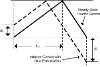 Figure 27. Effect of Initial Perturbation when dl1/dl0 < -1
dI1/dI0 can be calculated as:

The relationship between dI1/dI0 and K factor is illustrated graphically in the following.
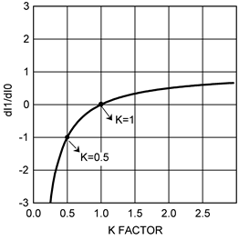 Figure 28. dl1/dl0 vs K Factor
The absolute minimum value of K is 0.5. When K < 0.5, the amplitude of dl1 is greater than the amplitude of dl0 and any initial perturbation results in sub-harmonic oscillation. If K=1, any initial perturbation will be removed in one switching cycle. This is known as one-cycle damping. When –1 < dl1/dl0 < 0, any initial perturbation will be under-damped. Any perturbation will be over-damped when 0 < dl1/dl0 < 1.
In the frequency-domain, Q, the quality factor of sampling gain term in modulator transfer function, is used to predict the tendency for sub-harmonic oscillation, which is defined as:

The relationship between Q and K factor is illustrated in Figure 29.
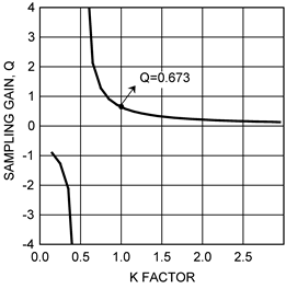 Figure 29. Sampling Gain Q vs K Factor
The recommended absolute minimum value of K is 0.5. High gain peaking when K is less than 0.5 results sub-harmonic oscillation at fSW/2. A higher value of K factor may introduce additional phase shift near the crossover frequency, but has the benefit of reducing noise susceptibility in current loop. The maximum allowable value of K factor can be calculated by the maximum crossover frequency equation in frequency analysis formulas in Table 2.
Table 2. Boost Regulator Frequency Analysis
| SIMPLIFIED FORMULA | COMPREHENSIVE FORMULA(1) | |
|---|---|---|
| MODULATOR TRANSER FUNCTION |
 |
 |
| Modulator DC gain (2) |
 |
|
| RHP zero (2) |
 |
|
| ESR zero |
 |
 |
| ESR pole | Not considered |
 |
| Dominant load pole |
 |
|
| Sampled gain inductor pole | Not considered |
  |
| Quality factor | Not considered |
 |
| Sub-harmonic double pole | Not considered |
 or  |
| K factor | K = 1 |
 |
| FEEDBACK TRANSFER FUNCTION |
 |
|
| Feedback DC gain |
 |
|
| Mid-band Gain |
 |
|
| Low frequency zero |
 |
|
| High frequency pole |
 |
 |
| OPEN LOOP RESPONSE |
 |
 |
| Crossover frequency (3)
(Open loop band width) |
 |
Use graphic tool |
| Maximum cross over frequency(4) |
 |
  |
 ,
,  ,
,  , and COUT = COUT of each phase x n, where n = number of phases.
  ,
,  ,
,  ,
,  , and
, and  .
.8.1.3 Interleaved Boost Configuration
Interleaved operation offers many advantages in single output, high current applications such as higher efficiency, lower component stresses and reduced input and output ripple. For dual phase interleaved operation, the output power path is split reducing the input current in each phase by one-half. Ripple currents in the input and output capacitors are reduced significantly since each channel operates 180 degrees out of phase from the other. Shown in Figure 30 is a normalized (IRMS/IOUT) output capacitor ripple current vs duty cycle for both a single phase and dual phase boost converter, where IRMS is the output current ripple RMS.
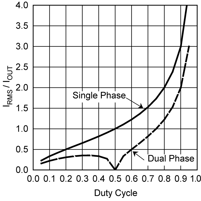 Figure 30. Normalized Output Capacitor RMS Ripple Current
To configure for dual phase interleaved operation, one device should be configured as a master and the other device should be configured in slave mode by connecting FB to VCC. Also COMP, UVLO, RES, SS and SYNCOUT on the master side should be connected to COMP, UVLO, RES, SS and SYNCIN on slave side respectively. The compensation network is connected between master FB and the common COMP connection. The output capacitors of the two power stages are connected together at the common output.
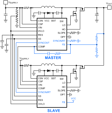 Figure 31. Dual Phase Interleaved Boost Configuration
Shown in Figure 32 is a dual phase timing diagram. The 180° phase shift is realized by connecting SYNCOUT on the master side to the SYNCIN on the slave side.
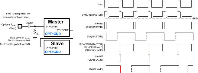 Figure 32. Dual Phase Configuration and Timing Diagram
Each channel is synchronized by an individual external clock in Figure 33. The SYNCOUT pin is used in Figure 34 requiring only one external clock source. A 50% duty cycle of external synchronization pulse should be always provided with this daisy chain configuration.
Current sharing between phases is achieved by sharing one error amplifier output of the master controller with the 3 slave controllers. Resistor sensing is a preferred method of current sensing to accurately balance the phase currents.
![LM25122-Q1 4-Phase Timing Diagram
Individual Clock LM25122-Q1 4 Phase Timing Diag [a].gif](/ods/images/ZHCSEL4A/4 Phase Timing Diag [a].gif) Figure 33. 4-Phase Timing Diagram Individual Clock
Figure 33. 4-Phase Timing Diagram Individual Clock
![LM25122-Q1 4-Phase Timing Diagram
Daisy Chain LM25122-Q1 4 Phase Timing Diag [b].gif](/ods/images/ZHCSEL4A/4 Phase Timing Diag [b].gif) Figure 34. 4-Phase Timing Diagram Daisy Chain
Figure 34. 4-Phase Timing Diagram Daisy Chain
8.1.4 DCR Sensing
For the applications requiring lowest cost with minimum conduction loss, Inductor DC resistance (DCR) is used to sense the inductor current rather than using a sense resistor. Shown in Figure 35 is a DCR sensing configuration using two DCR sensing resistors and one capacitor.
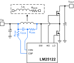 Figure 35. DCR Sensing
RCSN and CDCR selection should meet Equation 20 since this indirect current sensing method requires a time constant matching. CDCR is usually selected to be in the range of 0.1 µF to 2.2 µF.

Smaller value of RCSN minimizes the voltage drop caused by CSN bias current, but increases the dynamic power dissipation of RCSN. The DC voltage drop of RCSN can be compensated by selecting the same value of RCSP, but the gain of current amplifier, which is typically 10, is affected by adding RCSP. The gain of current amplifier with the DCR sensing network can be determined as:

Due to the reduced accuracy of DCR sensing, FPWM mode operation is recommended when DCR sensing is used.
8.1.5 Output Overvoltage Protection
Output overvoltage protection can be achieved by adding a simple external circuit. The output overvoltage protection circuit shown in Figure 36 shuts down the LM25122 when the output voltage exceeds the overvoltage threshold set by the zener diode.
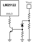 Figure 36. Output Overvoltage Protection
8.1.6 SEPIC Converter Simplified Schematic
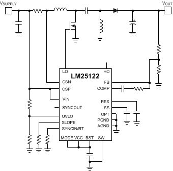 Figure 37. Sepic Converter Simplified Schematic
8.1.7 Non-Isolated Synchronous Flyback Converter Simplified Schematic
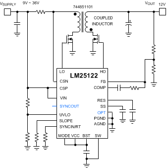 Figure 38. Non-Isolated Synchronous Flyback Converter Simplified Schematic
8.2 Typical Application
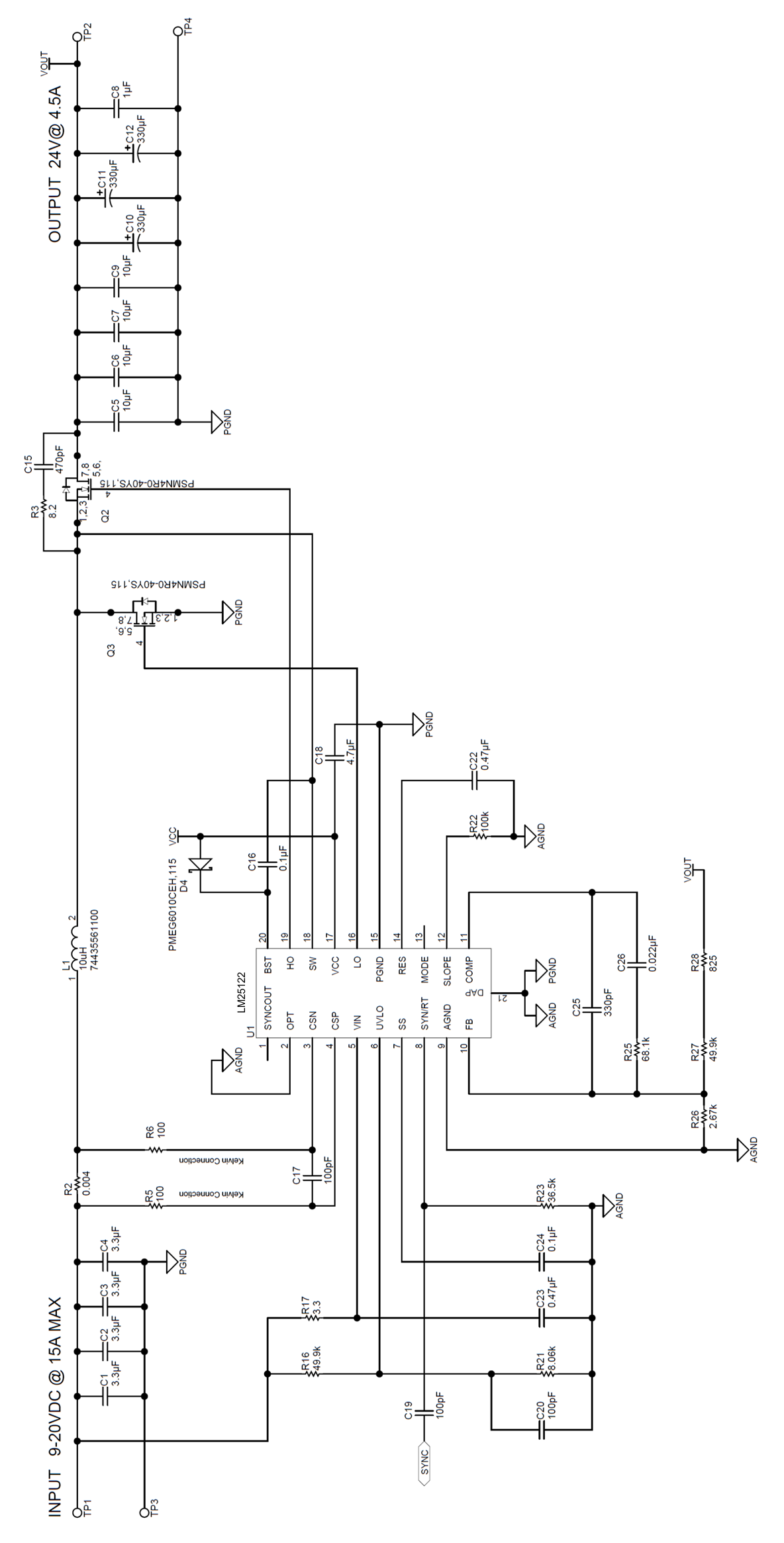 Figure 39. Single Phase Example Schematic
8.2.1 Design Requirements
| DESIGN PARAMETERS | VALUE |
|---|---|
| Output Voltage (VOUT) | 24 V |
| Full Load Current (IOUT) | 4.5 A |
| Output Power | 108 W |
| Minimum Input Voltage (VIN(MIN)) | 9 V |
| Typical Input Voltage (VIN(TYP)) | 12 V |
| Maximum Input Voltage (VIN(MAX)) | 20 V |
| Switching Frequency (fSW) | 250 kHz |
8.2.2 Detailed Design Procedure
8.2.2.1 Timing Resistor RT
Generally, higher frequency applications are smaller but have higher losses. Operation at 250 kHz is selected for this example as a reasonable compromise between small size and high-efficiency. The value of RT for 250 kHz switching frequency is calculated as follows:

A standard value of 36.5 kΩ is chosen for RT.
8.2.2.2 UVLO Divider RUV2, RUV1
The desired startup voltage and the hysteresis are set by the voltage divider RUV2, RUV1. The UVLO shutdown voltage should be high enough to enhance the low-side N-channel MOSFET switch fully. For this design, the startup voltage is set to 8.7 V which is 0.3 V below VIN(MIN). VHYS is set to 0.5 V. This results 8.2 V of VIN(SHUTDOWN). The values of RUV2, RUV1 are calculated as follows:


A standard value of 49.9 kΩ is selected for RUV2. RUV1 is selected to be a standard value of 8.06 kΩ.
8.2.2.3 Input Inductor LIN
The inductor ripple current is typically set between 20% and 40% of the full load current, known as a good compromise between core loss and copper loss of the inductor. Higher ripple current allows for a smaller inductor size, but places more of a burden on the output capacitor to smooth the ripple voltage on the output. For this example, a ripple ratio (RR) of 0.25, 25% of the input current was chosen. Knowing the switching frequency and the typical output voltage, the inductor value can be calculated as follows:

The closest standard value of 10 μH was chosen for LIN.
The saturation current rating of inductor should be greater than the peak inductor current, which is calculated at the minimum input voltage and full load. 8.7 V startup voltage is used conservatively.

8.2.2.4 Current Sense Resistor RS
The maximum peak input current capability should be 20~50% higher than the required peak current at low input voltage and full load, accounting for tolerances. For this example, 40% is margin is chosen.

A closest standard value of 4 mΩ is selected for RS. The maximum power loss of RS is calculated as follows.

8.2.2.5 Current Sense Filter RCSFP, RCSFN, CCS
The current sense filter is optional. 100 pF of CCS and 100 Ω of RCSFP, RCSFN are normal recommendations. Because CSP and CSN pins are high impedance, CCS should be placed physically as close to the device.
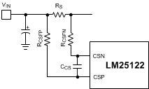 Figure 40. Current Sense Filter
8.2.2.6 Slope Compensation Resistor RSLOPE
The K value is selected to be 1 at the minimum input voltage. RSLOPE should be carefully selected so that the sum of sensed inductor current and slope compensation is less than COMP output high voltage.


A closest standard value of 100 kΩ is selected for RSLOPE.
8.2.2.7 Output Capacitor COUT
The output capacitors smooth the output voltage ripple and provide a source of charge during transient loading conditions. Also the output capacitors reduce the output voltage overshoot when the load is disconnected suddenly.
Ripple current rating of output capacitor should be carefully selected. In boost regulator, the output is supplied by discontinuous current and the ripple current requirement is usually high. In practice, the ripple current requirement can be dramatically reduced by placing high quality ceramic capacitors earlier than the bulk aluminum capacitors as close to the power switches.
The output voltage ripple is dominated by ESR of the output capacitors. Paralleling output capacitor is a good choice to minimize effective ESR and split the output ripple current into capacitors.
In this example, three 330 µF aluminum capacitors are used to share the output ripple current and source the required charge. The maximum output ripple current can be simply calculated at the minimum input voltage as follows:

Assuming 60 mΩ of ESR per an output capacitor, the output voltage ripple at the minimum input voltage is calculated as follows:

In practice, four 10 µF ceramic capacitors are additionally placed earlier than the bulk aluminum capacitors to reduce the output voltage ripple and split the output ripple current.
Due to the inherent path from input to output, unlimited inrush current can flow when the input voltage rises quickly and charges the output capacitor. The slew rate of input voltage rising should be controlled by a hot-swap or by starting the input power supply softly for the inrush current not to damage the inductor, sense resistor or high-side N-channel MOSFET switch.
8.2.2.8 Input Capacitor CIN
The input capacitors smooth the input voltage ripple. Assuming high quality ceramic capacitors are used for the input capacitors, the maximum input voltage ripple which happens when the input voltage is half of the output voltage can be calculated as follows:

The value of input capacitor is also a function of source impedance, the impedance of source power supply. The more input capacitor will be required to prevent a chatter condition upon power up if the impedance of source power supply is not enough low.
8.2.2.9 VIN Filter RVIN, CVIN
An R-C filter (RVIN, CVIN) on VIN pin is optional. It is not required if CIN capacitors are high quality ceramic capacitors and placed physically close to the device. The filter helps to prevent faults caused by high frequency switching noise injection into the VIN pin. A 0.47 μF ceramic capacitor is used this example. 3 Ω of RVIN and 0.47 µF of CVIN are normal recommendations. A larger filter with 2.2 µ~4.7 µF CVIN is recommended when the input voltage is lower than 8 V or the required duty cycle is close to the maximum duty cycle limit.
 Figure 41. VIN Filter
8.2.2.10 Bootstrap Capacitor CBST and Boost Diode DBST
The bootstrap capacitor between the BST and SW pin supplies the gate current to charge the high-side N-channel MOSFET device gate during each cycle’s turn-on and also supplies recovery charge for the bootstrap diode. These current peaks can be several amperes. The recommended value of the bootstrap capacitor is 0.1 μF. CBST should be a good quality, low ESR, ceramic capacitor located at the pins of the device to minimize potentially damaging voltage transients caused by trace inductance. The minimum value for the bootstrap capacitor is calculated as follows:

Where QG is the high-side N-channel MOSFET gate charge and ΔVBST is the tolerable voltage droop on CBST, which is typically less than 5% of VCC or 0.15 V, conservatively. In this example, the value of the BST capacitor (CBST) is 0.1 µF.
The voltage rating of DBST should be greater than the peak SW node voltage plus 16 V. A low leakage diode is mandatory for the bypass operation. The leakage current of DBST should be low enough for the BST charge pump to maintain a sufficient high-side driver supply voltage at high temperature. A low leakage diode also prevents the possibility of excessive VCC voltage during shutdown, in high output voltage applications. If the leakage is excessive, a zener VCC clamp or bleed resistor may be required. High-side driver supply voltage should be greater than the high-side N-channel MOSFET switch’s gate plateau at the minimum input voltage.
8.2.2.11 VCC Capacitor CVCC
The primary purpose of the VCC capacitor is to supply the peak transient currents of the LO driver and bootstrap diode as well as provide stability for the VCC regulator. These peak currents can be several amperes. The value of CVCC should be at least 10 times greater than the value of CBST, and should be a good quality, low ESR, ceramic capacitor. CVCC should be placed close to the pins of the IC to minimize potentially damaging voltage transients caused by trace inductance. A value of 4.7 µF was selected for this design example.
8.2.2.12 Output Voltage Divider RFB1, RFB2
RFB1 and RFB2 set the output voltage level. The ratio of these resistors is calculated as follows:

The ratio between RCOMP and RFB2 determines the mid-band gain, AFB_MID. A larger value for RFB2 may require a corresponding larger value for RCOMP. RFB2 should be large enough to keep the total divider power dissipation small. 49.9 kΩ in series with 825 Ω was chosen for high-side feedback resistors in this example, which results in a RFB1 value of 2.67 kΩ for 24 V output.
8.2.2.13 Soft-Start Capacitor CSS
The soft-start time (tSS) is the time for the output voltage to reach the target voltage from the input voltage. The soft-start time is not only proportional with the soft-start capacitor, but also depends on the input voltage. With 0.1 µF of CSS, the soft-start time is calculated as follows:


8.2.2.14 Restart Capacitor CRES
The restart capacitor determines restart delay time tRD and hiccup mode off time tRES (see Figure 26). tRD should be greater than tSS(MAX). The minimum required value of CRES can be calculated at the low input voltage as follows:

A standard value of 0.47 µF is selected for CRES.
8.2.2.15 Low-Side Power Switch QL
Selection of the power N-channel MOSFET devices by breaking down the losses is one way to compare the relative efficiencies of different devices. Losses in the low-side N-channel MOSFET device can be separated into conduction loss and switching loss.
Low-side conduction loss is approximately calculated as follows:

Where, D is the duty cycle and the factor of 1.3 accounts for the increase in the N-channel MOSFET device on-resistance due to heating. Alternatively, the factor of 1.3 can be eliminated and the high temperature on-resistance of the N-channel MOSFET device can be estimated using the RDS(ON) vs temperature curves in the N-channel MOSFET datasheet.
Switching loss occurs during the brief transition period as the low-side N-channel MOSFET device turns on and off. During the transition period both current and voltage are present in the channel of the N-channel MOSFET device. The low-side switching loss is approximately calculated as follows:

tR and tF are the rise and fall times of the low-side N-channel MOSFET device. The rise and fall times are usually mentioned in the N-channel MOSFET datasheet or can be empirically observed with an oscilloscope.
An additional Schottky diode can be placed in parallel with the low-side N-channel MOSFET switch, with short connections to the source and drain in order to minimize negative voltage spikes at the SW node.
8.2.2.16 High-Side Power Switch QH and Additional Parallel Schottky Diode
Losses in the high-side N-channel MOSFET device can be separated into conduction loss, dead-time loss and reverse recovery loss. Switching loss is calculated for the low-side N-channel MOSFET device only. Switching loss in the high-side N-channel MOSFET device is negligible because the body diode of the high-side N-channel MOSFET device turns on before and after the high-side N-channel MOSFET device switches.
High-side conduction loss is approximately calculated as follows:

Dead-time loss is approximately calculated as follows:

where
- VD is the forward voltage drop of the high-side NMOS body diode.
Reverse recovery characteristics of the high-side N-channel MOSFET switch strongly affect efficiency, especially when the output voltage is high. Small reverse recovery charge helps to increase the efficiency while also minimizes switching noise.
Reverse recovery loss is approximately calculated as follows:

where
- QRR is the reverse recovery charge of the high-side N-channel MOSFET body diode.
An additional Schottky diode can be placed in parallel with the high-side switch to improve efficiency. Usually, the power rating of this parallel Schottky diode can be less than the high-side switch’s because the diode conducts only during dead-times. The power rating of the parallel diode should be equivalent or higher than high-side switch’s if bypass operation is required, hiccup mode operation is required or any load exists before switching.
8.2.2.17 Snubber Components
A resistor-capacitor snubber network across the high-side N-channel MOSFET device reduces ringing and spikes at the switching node. Excessive ringing and spikes can cause erratic operation and can couple noise to the output voltage. Selecting the values for the snubber is best accomplished through empirical methods. First, make sure the lead lengths for the snubber connections are very short. Start with a resistor value between 5 and 50 Ω. Increasing the value of the snubber capacitor results more damping, but this also results higher snubber losses. Select a minimum value for the snubber capacitor that provides adequate damping of the spikes on the switch waveform at heavy load. A snubber may not be necessary with an optimized layout.
8.2.2.18 Loop Compensation Components CCOMP, RCOMP, CHF
RCOMP, CCOMP and CHF configure the error amplifier gain and phase characteristics to produce a stable voltage loop. For a quick start, follow the following 4 steps:
- Select fCROSS
- Determine required RCOMP
- Determine CCOMP to cancel load pole. Place error amplifier zero at the twice of load pole frequency. Knowing RCOMP, CCOMP is calculated as follows:
- Determine CHF to cancel ESR zero.
Select the cross over frequency (fCROSS) at one fourth of the RHP zero or one tenth of the switching frequency whichever is lower.


5.3 kHz of the crossover frequency is selected between two. RHP zero at minimum input voltage should be considered if the input voltage range is wide.
Knowing fCROSS, RCOMP is calculated as follows:

A standard value of 68.1 kΩ is selected for RCOMP

A standard value of 22 nF is selected for CCOMP
Knowing RCOMP, RESR and CCOMP, CHF is calculated as follows:

A standard value of 330 pF is selected for CHF.
8.2.3 Application Curves
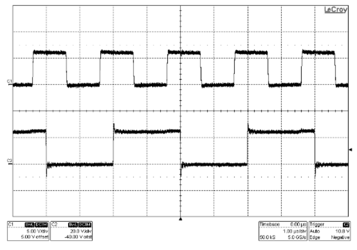
| C1: FSYNC , C2: SW | VSUPPLY = 12 V, FSYNC = 500 kHz |
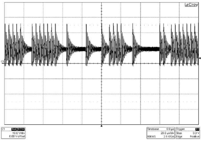
| C1:SW | VSUPPLY = 12 V, ILOAD = 0A |
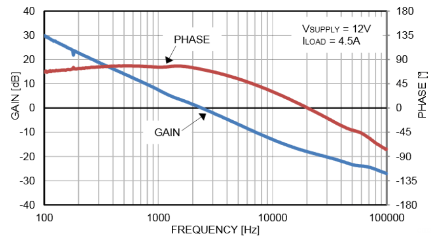
| C1:SW | VSUPPLY = 12 V, ILOAD = 0A |
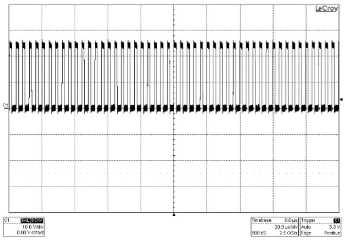
| C1:SW | VSUPPLY = 12 V, ILOAD = 0A |
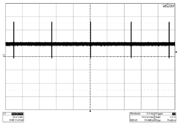
| C1:SW | VSUPPLY = 12 V, ILOAD = 0A |
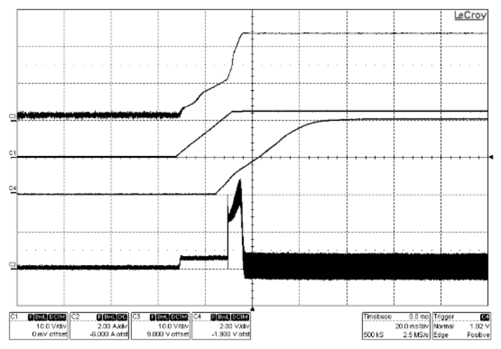
| C1: VSUPPLY, C2: Inductor current, C3: VOUT, C4: SS | VSUPPLY = 12 V, ILOAD = 0A | |


