ZHCSG23A March 2017 – February 2018 LM25141-Q1
PRODUCTION DATA.
- 1 特性
- 2 应用
- 3 说明
- 4 修订历史记录
- 5 Pin Configuration and Functions
- 6 Specifications
-
7 Detailed Description
- 7.1 Overview
- 7.2 Functional Block Diagram
- 7.3
Feature Description
- 7.3.1 High Voltage Start-Up Regulator
- 7.3.2 VCC Regulator
- 7.3.3 Oscillator
- 7.3.4 Synchronization
- 7.3.5 Frequency Dithering (Spread Spectrum)
- 7.3.6 Enable
- 7.3.7 Power Good
- 7.3.8 Output Voltage
- 7.3.9 Current Sense
- 7.3.10 DCR Current Sensing
- 7.3.11 Error Amplifier and PWM Comparator
- 7.3.12 Slope Compensation
- 7.3.13 Hiccup Mode Current Limiting
- 7.3.14 Standby Mode
- 7.3.15 Soft Start
- 7.3.16 Diode Emulation
- 7.3.17 High- and Low-Side Drivers
-
8 Application and Implementation
- 8.1 Application Information
- 8.2 Typical Application
- 9 Power Supply Recommendations
- 10Layout
- 11器件和文档支持
- 12机械、封装和可订购信息
封装选项
机械数据 (封装 | 引脚)
- RGE|24
散热焊盘机械数据 (封装 | 引脚)
- RGE|24
订购信息
8.2.2.6.1 Feedback Compensator
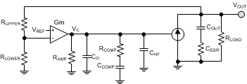
A type II compensator using an transconductance error amplifier (EA), Gm, is shown in Figure 35. The dominant pole of the EA open-loop gain is set by the EA output resistance, RAMP, and effective bandwidth-limiting capacitance, CO, as follows:

The EA high frequency pole is neglected in the above expression. The compensator transfer function from output voltage to COMP, including the gain contribution from the feedback resistor divider network is:


where
Which simplifies to:
 Figure 35. Transconductance Amplifier


Typically RCOMP<< RAMP and CCOMP>> (CHF + CO) so the approximations are valid.
where
VREF is the feedback voltage reference (1.2 V)
Gm is the error amplifier gain transconductance (1200 µS)
RAMP is the error amplifier output impedance (2.5 MΩ)
The error amplifier compensation components create a pole at the origin, a zero, and a high frequency pole.
The procedure for choosing compensation components for a stable closed loop is:
- Select the desired open-loop gain crossover frequency (fc); for this application 30 kHz was chosen
- Calculate the RCOMP resistor for the gain crossover frequency at 30 kHz
- Calculate the CCOMP capacitor value to create a zero that cancels the pole ωp (ωp = 1/RLOAD × COUT)


The value selected for RCOMP is 22.6 kΩ.
where
RDCR = 0.0081 Ω


The value selected for CCOMP is 10 nF.
