ZHCSLO7B December   2020  – January 2023 LM25149-Q1

PRODUCTION DATA  

  1. 特性
  2. 应用
  3. 说明
  4. Revision History
  5. 说明(续)
  6. Pin Configuration and Functions
    1. 6.1 Wettable Flanks
  7. Specifications
    1. 7.1 Absolute Maximum Ratings
    2. 7.2 ESD Ratings 
    3. 7.3 Recommended Operating Conditions
    4. 7.4 Thermal Information
    5. 7.5 Electrical Characteristics
    6. 7.6 Active EMI Filter
    7. 7.7 Typical Characteristics
  8. Detailed Description
    1. 8.1 Overview
    2. 8.2 Functional Block Diagram
    3. 8.3 Feature Description
      1. 8.3.1  Input Voltage Range (VIN)
      2. 8.3.2  High-Voltage Bias Supply Regulator (VCC, VCCX, VDDA)
      3. 8.3.3  Precision Enable (EN)
      4. 8.3.4  Power-Good Monitor (PG)
      5. 8.3.5  Switching Frequency (RT)
      6. 8.3.6  Active EMI Filter
      7. 8.3.7  Dual Random Spread Spectrum (DRSS)
      8. 8.3.8  Soft Start
      9. 8.3.9  Output Voltage Setpoint (FB)
      10. 8.3.10 Minimum Controllable On Time
      11. 8.3.11 Error Amplifier and PWM Comparator (FB, EXTCOMP)
      12. 8.3.12 Slope Compensation
      13. 8.3.13 Inductor Current Sense (ISNS+, VOUT)
        1. 8.3.13.1 Shunt Current Sensing
        2. 8.3.13.2 Inductor DCR Current Sensing
      14. 8.3.14 Hiccup Mode Current Limiting
      15. 8.3.15 High-Side and Low-Side Gate Drivers (HO, LO)
      16. 8.3.16 Output Configurations (CNFG)
      17. 8.3.17 Single-Output Dual-Phase Operation
    4. 8.4 Device Functional Modes
      1. 8.4.1 Sleep Mode
      2. 8.4.2 Pulse Frequency Modulation and Synchronization (PFM/SYNC)
      3. 8.4.3 Thermal Shutdown
  9. Application and Implementation
    1. 9.1 Application Information
      1. 9.1.1 Power Train Components
        1. 9.1.1.1 Buck Inductor
        2. 9.1.1.2 Output Capacitors
        3. 9.1.1.3 Input Capacitors
        4. 9.1.1.4 Power MOSFETs
        5. 9.1.1.5 EMI Filter
        6. 9.1.1.6 Active EMI Filter
      2. 9.1.2 Error Amplifier and Compensation
    2. 9.2 Typical Applications
      1. 9.2.1 Design 1 – High-Efficiency 2.1-MHz Synchronous Buck Regulator
        1. 9.2.1.1 Design Requirements
        2. 9.2.1.2 Detailed Design Procedure
          1. 9.2.1.2.1  Custom Design With WEBENCH® Tools
          2. 9.2.1.2.2  Custom Design With Excel Quickstart Tool
          3. 9.2.1.2.3  Buck Inductor
          4. 9.2.1.2.4  Current-Sense Resistance
          5. 9.2.1.2.5  Output Capacitors
          6. 9.2.1.2.6  Input Capacitors
          7. 9.2.1.2.7  Frequency Set Resistor
          8. 9.2.1.2.8  Feedback Resistors
          9. 9.2.1.2.9  Compensation Components
          10. 9.2.1.2.10 Active EMI Components
        3. 9.2.1.3 Application Curves
      2. 9.2.2 Design 2 – High Efficiency 440-kHz Synchronous Buck Regulator
        1. 9.2.2.1 Design Requirements
        2. 9.2.2.2 Detailed Design Procedure
        3. 9.2.2.3 Application Curves
      3. 9.2.3 Design 3 – Dual-Phase 400-kHz 20-A Synchronous Buck Regulator
        1. 9.2.3.1 Design Requirements
        2. 9.2.3.2 Detailed Design Procedure
        3. 9.2.3.3 Application Curves
    3. 9.3 Power Supply Recommendations
    4. 9.4 Layout
      1. 9.4.1 Layout Guidelines
        1. 9.4.1.1 Power Stage Layout
        2. 9.4.1.2 Gate-Drive Layout
        3. 9.4.1.3 PWM Controller Layout
        4. 9.4.1.4 Active EMI Layout
        5. 9.4.1.5 Thermal Design and Layout
        6. 9.4.1.6 Ground Plane Design
      2. 9.4.2 Layout Example
  10. 10Device and Documentation Support
    1. 10.1 Device Support
      1. 10.1.1 Development Support
        1. 10.1.1.1 Custom Design With WEBENCH® Tools
    2. 10.2 Documentation Support
      1. 10.2.1 Related Documentation
        1. 10.2.1.1 PCB Layout Resources
        2. 10.2.1.2 Thermal Design Resources
    3. 10.3 接收文档更新通知
    4. 10.4 支持资源
    5. 10.5 Trademarks
    6. 10.6 静电放电警告
    7. 10.7 术语表
  11. 11Mechanical, Packaging, and Orderable Information

封装选项

机械数据 (封装 | 引脚)
散热焊盘机械数据 (封装 | 引脚)
订购信息

Application Curves

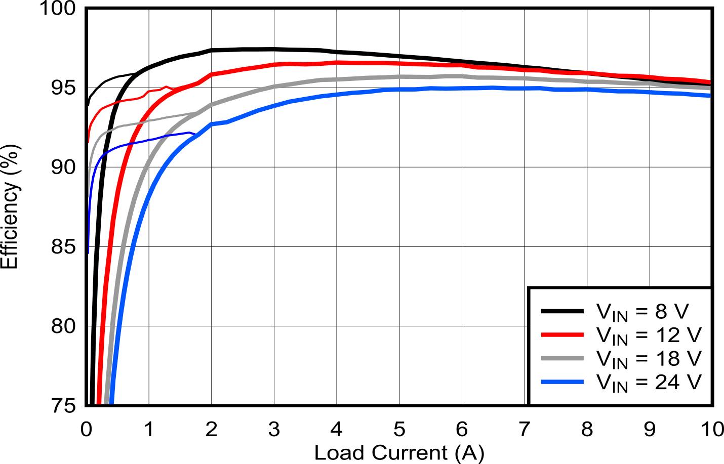
GUID-D6428CFF-5559-4660-9C9B-BB0C6C3F4E73-low.png
5-V output
Figure 9-19 Efficiency vs. IOUT
10-A resistive load
Figure 9-21 Full load Switching
VIN ramps from 12 to 40 V 5-A load
Figure 9-23 Line Transient Response to VIN = 40 V
VIN step to 12 V 10-A resistive load
Figure 9-25 Start-Up Characteristic
VIN = 12 V FPWM
Figure 9-27 Load Transient, 0 A to 10 A
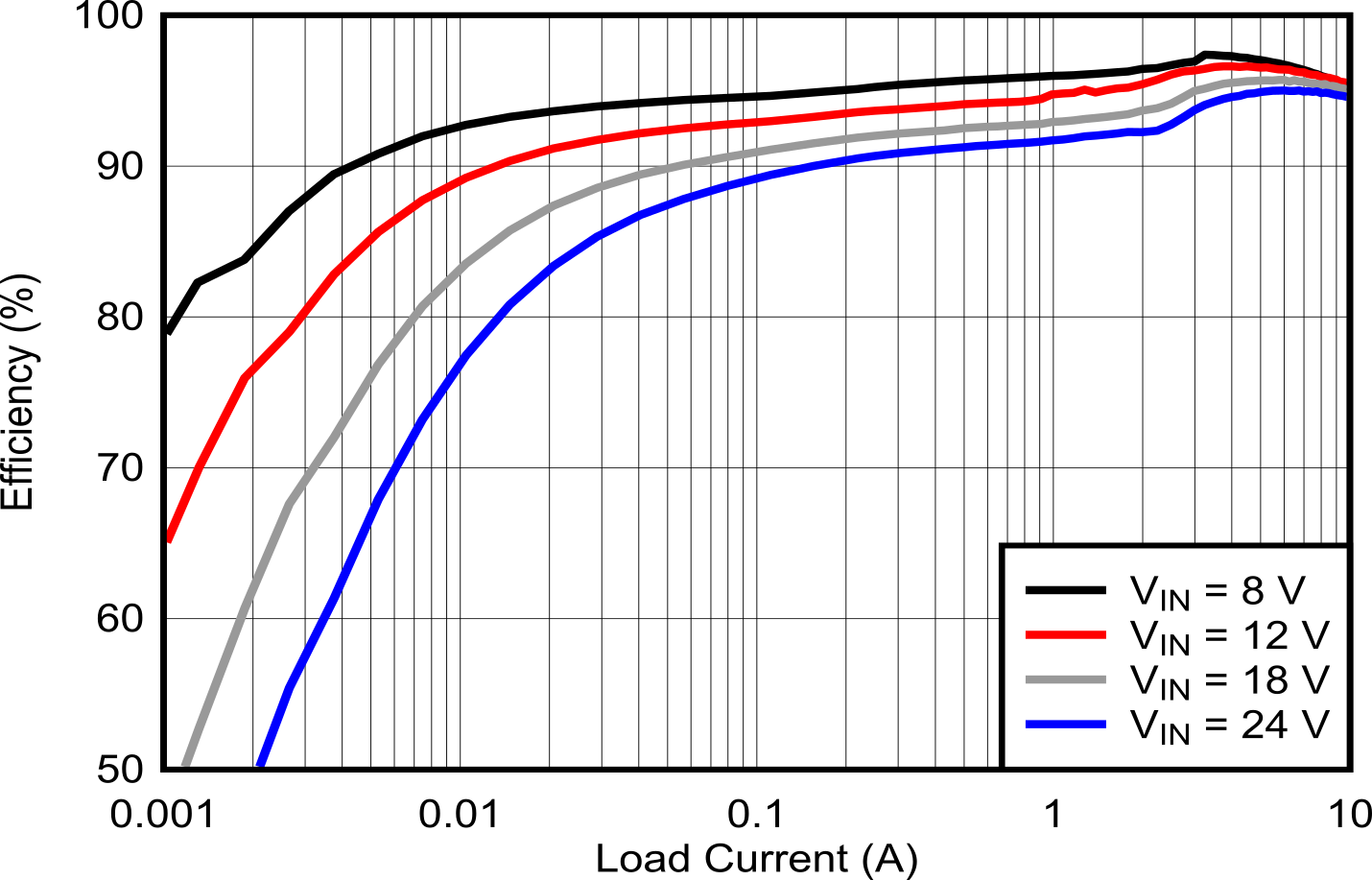
GUID-5420C7A7-A97B-4C90-851D-7C32FFCA2A4E-low.png
5-V output
Figure 9-20 Efficiency vs. IOUT, Log Scale
No load
Figure 9-22 PFM Switching
VIN falls to 4 V 1-A load
Figure 9-24 Cold-Crank Response to VIN = 4 V
VIN = 12 V 10-A resistive load
Figure 9-26 ENABLE ON and OFF Characteristic
VIN = 12 V FPWM
Figure 9-28 Load Transient, 5 A to 10 A