ZHCSLO5B December 2020 – December 2021 LM25149
PRODUCTION DATA
- 1 特性
- 2 应用
- 3 说明
- 4 Revision History
- 5 说明(续)
- 6 Pin Configuration and Functions
- 7 Specifications
-
8 Detailed Description
- 8.1 Overview
- 8.2 Functional Block Diagram
- 8.3
Feature Description
- 8.3.1 Input Voltage Range (VIN)
- 8.3.2 High-Voltage Bias Supply Regulator (VCC, VCCX, VDDA)
- 8.3.3 Precision Enable (EN)
- 8.3.4 Power-Good Monitor (PG)
- 8.3.5 Switching Frequency (RT)
- 8.3.6 Active EMI Filter
- 8.3.7 Dual Random Spread Spectrum (DRSS)
- 8.3.8 Soft Start
- 8.3.9 Output Voltage Setpoint (FB)
- 8.3.10 Minimum Controllable On Time
- 8.3.11 Error Amplifier and PWM Comparator (FB, EXTCOMP)
- 8.3.12 Slope Compensation
- 8.3.13 Inductor Current Sense (ISNS+, VOUT)
- 8.3.14 Hiccup Mode Current Limiting
- 8.3.15 High-Side and Low-Side Gate Drivers (HO, LO)
- 8.3.16 Output Configurations (CNFG)
- 8.3.17 Single-Output Dual-Phase Operation
- 8.4 Device Functional Modes
-
9 Application and Implementation
- 9.1 Application Information
- 9.2
Typical Applications
- 9.2.1
Design 1 – High Efficiency 2.1-MHz Synchronous
Buck Regulator
- 9.2.1.1 Design Requirements
- 9.2.1.2
Detailed Design Procedure
- 9.2.1.2.1 Custom Design With WEBENCH® Tools
- 9.2.1.2.2 Custom Design With Excel Quickstart Tool
- 9.2.1.2.3 Buck Inductor
- 9.2.1.2.4 Current-Sense Resistance
- 9.2.1.2.5 Output Capacitors
- 9.2.1.2.6 Input Capacitors
- 9.2.1.2.7 Frequency Set Resistor
- 9.2.1.2.8 Feedback Resistors
- 9.2.1.2.9 Compensation Components
- 9.2.1.2.10 Active EMI Components
- 9.2.1.3 Application Curves
- 9.2.2 Design 2 – High Efficiency 440-kHz Synchronous Buck Regulator
- 9.2.3 Design 3 – Dual-Phase 400-kHz 20-A Synchronous Buck Regulator
- 9.2.1
Design 1 – High Efficiency 2.1-MHz Synchronous
Buck Regulator
- 10Power Supply Recommendations
- 11Layout
- 12Device and Documentation Support
- 13Mechanical, Packaging, and Orderable Information
11.2 Layout Example
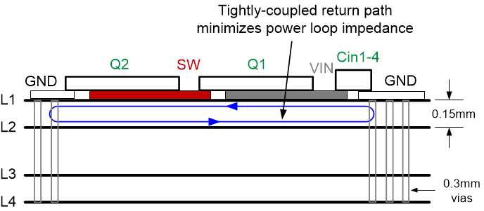
Figure 11-2 shows a single-sided layout of a synchronous buck regulator with discrete power MOSFETs, Q1 and Q2, in SON 5-mm × 6-mm case size. The power stage is surrounded by a GND pad geometry to connect an EMI shield if needed. The design uses layer 2 of the PCB as a power-loop return path directly underneath the top layer to create a low-area switching power loop of approximately 2 mm². This loop area, and hence parasitic inductance, must be as small as possible to minimize EMI as well as switch-node voltage overshoot and ringing.
The high-frequency power loop current flows through MOSFETs Q1 and Q2, through the power ground plane on layer 2, and back to VIN through the 0402 ceramic capacitors C17 through C22. The currents flowing in opposing directions in the vertical loop configuration provide field self-cancellation, reducing parasitic inductance. Figure 11-4 shows a side view to illustrate the concept of creating a low-profile, self-canceling loop in a multilayer PCB structure. The layer-2 GND plane layer, shown in Figure 11-3, provides a tightly-coupled current return path directly under the MOSFETs to the source terminals of Q2.
Six 10-nF input capacitors with small 0402 or 0603 case size are placed in parallel very close to the drain of Q1. The low equivalent series inductance (ESL) and high self-resonant frequency (SRF) of the small footprint capacitors yield excellent high-frequency performance. The negative terminals of these capacitors are connected to the layer-2 GND plane with multiple 12-mil (0.3-mm) diameter vias, further minimizing parasitic loop inductance.
Additional guidelines to improve noise immunity and reduce EMI are as follows:
- Make the ground connections to the LM25149 controller as shown in Figure 11-2. Create a power ground directly connected to all high-power components and an analog ground plane for sensitive analog components. The analog ground plane for AGND and power ground plane for PGND must be connected at a single point directly under the IC – at the die attach pad (DAP).
- Connect the MOSFETs (switch node) directly to the inductor terminal with short copper connections (without vias) as this net has high dv/dt and contributes to radiated EMI. The single-layer routing of the switch-node connection means that switch-node vias with high dv/dt do not appear on the bottom side of the PCB. This avoids e-field coupling to the reference ground plane during the EMI test. VIN and PGND plane copper pours shield the polygon connecting the MOSFETs to the inductor terminal, further reducing the radiated EMI signature.
- Place the EMI filter components on the bottom side of the PCB so that they are shielded from the power stage components on the top side.
 Figure 11-4 PCB Stack-up
Diagram With Low L1-L2 Intra-layer Spacing (1)