ZHCS529H January   2007  – August 2017 LM25574

PRODUCTION DATA.  

  1. 特性
  2. 应用
  3. 说明
    1.     Device Images
      1.      简化应用电路原理图
  4. 修订历史记录
  5. Pin Configuration and Functions
    1.     Pin Functions
  6. Specifications
    1. 6.1 Absolute Maximum Ratings
    2. 6.2 ESD Ratings
    3. 6.3 Recommended Operating Conditions
    4. 6.4 Thermal Information
    5. 6.5 Electrical Characteristics
    6. 6.6 Typical Characteristics
  7. Detailed Description
    1. 7.1 Overview
    2. 7.2 Functional Block Diagram
    3. 7.3 Feature Description
      1. 7.3.1 High Voltage Start-Up Regulator
    4. 7.4 Device Functional Modes
      1. 7.4.1 Shutdown and Stand-by Mode
      2. 7.4.2 Oscillator and Sync Capability
      3. 7.4.3 Error Amplifier and PWM Comparator
      4. 7.4.4 Ramp Generator
      5. 7.4.5 Maximum Duty Cycle and Input Drop-out Voltage
      6. 7.4.6 Current Limit
      7. 7.4.7 Soft-Start
      8. 7.4.8 Boost Pin
      9. 7.4.9 Thermal Protection
  8. Application and Implementation
    1. 8.1 Application Information
      1. 8.1.1  External Components
      2. 8.1.2  R3 (RT)
      3. 8.1.3  L1
      4. 8.1.4  C3 (CRAMP)
      5. 8.1.5  C9
      6. 8.1.6  C1
      7. 8.1.7  C8
      8. 8.1.8  C7
      9. 8.1.9  C4
      10. 8.1.10 R5, R6
      11. 8.1.11 R1, R2, C2
      12. 8.1.12 R4, C5, C6
      13. 8.1.13 Bias Power Dissipation Reduction
    2. 8.2 Typical Application
      1. 8.2.1 Typical Schematic for High Frequency (1MHz) Application
      2. 8.2.2 Detailed Design Procedure
        1. 8.2.2.1 Custom Design With WEBENCH® Tools
  9. Layout
    1. 9.1 Layout Guidelines
      1. 9.1.1 PCB Layout and Thermal Considerations
    2. 9.2 Layout Example
  10. 10器件和文档支持
    1. 10.1 器件支持
      1. 10.1.1 开发支持
        1. 10.1.1.1 使用 WEBENCH® 工具创建定制设计
    2. 10.2 接收文档更新通知
    3. 10.3 社区资源
    4. 10.4 商标
    5. 10.5 静电放电警告
    6. 10.6 Glossary
  11. 11机械、封装和可订购信息

封装选项

机械数据 (封装 | 引脚)
散热焊盘机械数据 (封装 | 引脚)
订购信息

L1

The inductor value is determined based on the operating frequency, load current, ripple current, and the minimum and maximum input voltage (VIN(min), VIN(max)).
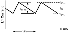
LM25574 20214110.gifFigure 14. Inductor Current Waveform

To keep the circuit in continuous conduction mode (CCM), the maximum ripple current IRIPPLE should be less than twice the minimum load current, or 0.2 Ap-p. Using this value of ripple current, the value of inductor (L1) is calculated using the following:

Equation 6. LM25574 20214111.gif
Equation 7. LM25574 20214112.gif

This procedure provides a guide to select the value of L1. The nearest standard value (100µH) will be used. L1 must be rated for the peak current (IPK+) to prevent saturation. During normal loading conditions, the peak current occurs at maximum load current plus maximum ripple. During an overload condition the peak current is limited to 0.7A nominal (0.85A maximum). The selected inductor (see Table 1) has a conservative 1.0 Amp saturation current rating. For this manufacturer, the saturation rating is defined as the current necessary for the inductance to reduce by 30%, at 20°C.