ZHCSIJ1E June 1999 – July 2018 LM2574 , LM2574HV
PRODUCTION DATA.
- 1 特性
- 2 应用
- 3 说明
- 4 修订历史记录
- 5 Pin Configuration and Functions
-
6 Specifications
- 6.1 Absolute Maximum Ratings
- 6.2 ESD Ratings
- 6.3 Recommended Operating Conditions
- 6.4 Thermal Information
- 6.5 Electrical Characteristics for All Output Voltage Versions
- 6.6 Electrical Characteristics – 3.3-V Version
- 6.7 Electrical Characteristics – 5-V Version
- 6.8 Electrical Characteristics – 12-V Version
- 6.9 Electrical Characteristics – 15-V Version
- 6.10 Electrical Characteristics – Adjustable Version
- 6.11 Typical Characteristics
- 7 Detailed Description
-
8 Application and Implementation
- 8.1 Application Information
- 8.2 Typical Applications
- 9 Power Supply Recommendations
- 10Layout
- 11器件和文档支持
- 12机械、封装和可订购信息
8.1.9.1 Inverting Regulator
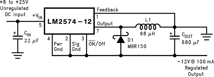
Figure 20 shows a LM2574-12 in a buck-boost configuration to generate a negative 12-V output from a positive input voltage. This circuit bootstraps the ground pin of the regulator to the negative output voltage, then by grounding the feedback pin, the regulator senses the inverted output voltage and regulates it to −12 V.

For an input voltage of 8 V or more, the maximum available output current in this configuration is approximately 100 mA. At lighter loads, the minimum input voltage required drops to approximately 4.7 V.
The switch currents in this buck-boost configuration are higher than in the standard buck-mode design, thus lowering the available output current. Also, the start-up input current of the buck-boost converter is higher than the standard buck-mode regulator, and this may overload an input power source with a current limit less than
0.6 A. Using a delayed turnon or an undervoltage lockout circuit (described in Negative Boost Regulator) would allow the input voltage to rise to a high enough level before the switcher would be allowed to turn on.
Because of the structural differences between the buck and the buck-boost regulator topologies, the design procedure can not be used to select the inductor or the output capacitor. The recommended range of inductor values for the buck-boost design is between 68 μH and 220 μH, and the output capacitor values must be larger than what is normally required for buck designs. Low-input voltages or high-output currents require a large value output capacitor (in the thousands of micro Farads).
The peak inductor current, which is the same as the peak switch current, can be calculated from Equation 6.

where
- fosc = 52 kHz. Under normal continuous inductor current operating conditions,
- the minimum VIN represents the worst case. Select an inductor that is rated for the peak current anticipated.
Also, the maximum voltage appearing across the regulator is the absolute sum of the input and output voltage. For a −12-V output, the maximum input voltage for the LM2574 is 28 V, or 48 V for the LM2574HV.