SLVS569F January 2005 – August 2015 LM2575
PRODUCTION DATA.
- 1 Features
- 2 Applications
- 3 Description
- 4 Revision History
- 5 Pin Configuration and Functions
- 6 Specifications
- 7 Detailed Description
-
8 Application and Implementation
- 8.1 Application Information
- 8.2
Typical Application
- 8.2.1 Design Requirements
- 8.2.2
Detailed Design Procedure
- 8.2.2.1 Input Capacitor (CIN)
- 8.2.2.2 Output Capacitor (COUT)
- 8.2.2.3 Catch Diode
- 8.2.2.4 Inductor
- 8.2.2.5 Output Voltage Ripple and Transients
- 8.2.2.6 Feedback Connection
- 8.2.2.7 ON/OFF Input
- 8.2.2.8 Grounding
- 8.2.2.9 Reverse Current Considerations
- 8.2.2.10 Buck Regulator Design Procedure
- 8.2.2.11 Inductor Selection Guide
- 8.2.3 Application Curves
- 9 Power Supply Recommendations
- 10Layout
- 11Device and Documentation Support
- 12Mechanical, Packaging, and Orderable Information
10 Layout
10.1 Layout Guidelines
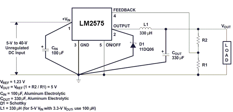
With any switching regulator, circuit layout plays an important role in circuit performance. Wiring and parasitic inductances, as well as stray capacitances, are subjected to rapidly switching currents, which can result in unwanted voltage transients. To minimize inductance and ground loops, the length of the leads indicated by heavy lines (see Figure 16) must be minimized. Optimal results can be achieved by single-point grounding or by ground-plane construction. For the same reasons, the two programming resistors used in the adjustable version must be located as close as possible to the regulator to keep the sensitive feedback wiring short.
 Figure 16. Test Circuit and Layout Guidelines
10.2 Layout Example
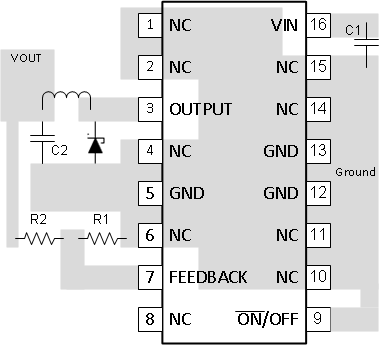
The large ground copper area helps heat transfer especially when many vias to ground plane are used.
 Figure 17. Layout Diagram